Cayden Doyle, Sandeep Dhakal, Allyssa Bateman, Dr. Indrajit Charit, Mark Jaster, Dr. Brian Jaques.
Introduction
The laser additive manufacturing (AM) process of 316 stainless steel (SS) undergoes rapid heating and results in non-uniform cooling, causing a significant change in the microstructure and producing residual stresses.
A major focus of this project was evaluating the grain morphology, chemical homogeneity, and the crystallographic texture to improve the performance of AM metals.
Experimental Procedure
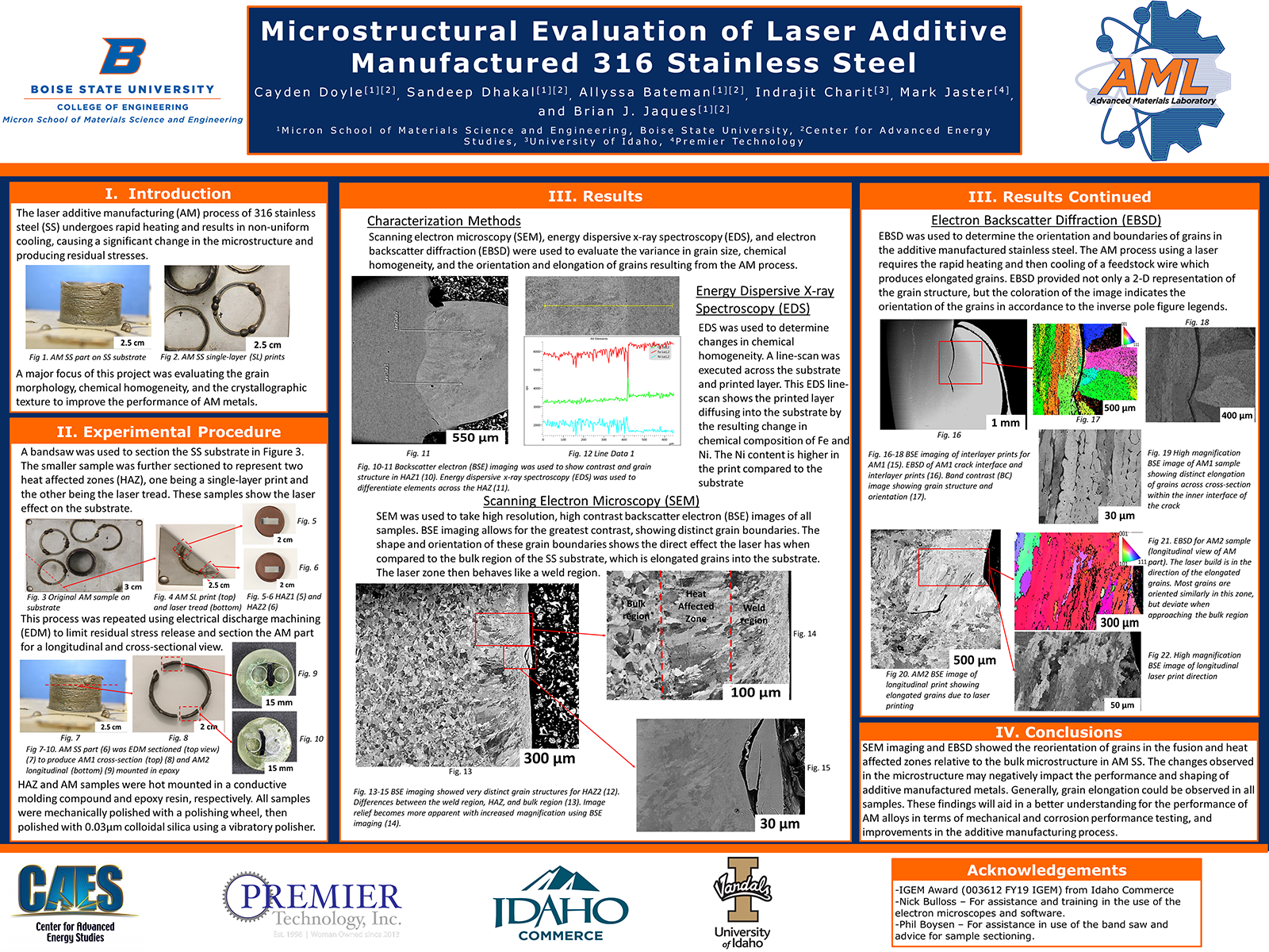
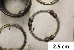
A bandsaw was used to section the SS substrate in Figure 3. The smaller sample was further sectioned to represent two heat affected zones (HAZ), one being a single-layer print and the other being the laser tread. These samples show the laser effect on the substrate.

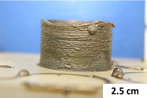
This process was repeated using electrical discharge machining (EDM) to limit residual stress release and section the AM part for a longitudinal and cross-sectional view.
HAZ and AM samples were hot mounted in a conductive molding compound and epoxy resin, respectively. All samples were mechanically polished with a polishing wheel, then polished with 0.03μm colloidal silica using a vibratory polisher.
Results
Characterization Methods
Scanning electron microscopy (SEM), energy dispersive x-ray spectroscopy (EDS), and electron backscatter diffraction (EBSD) were used to evaluate the variance in grain size, chemical homogeneity, and the orientation and elongation of grains resulting from the AM process.
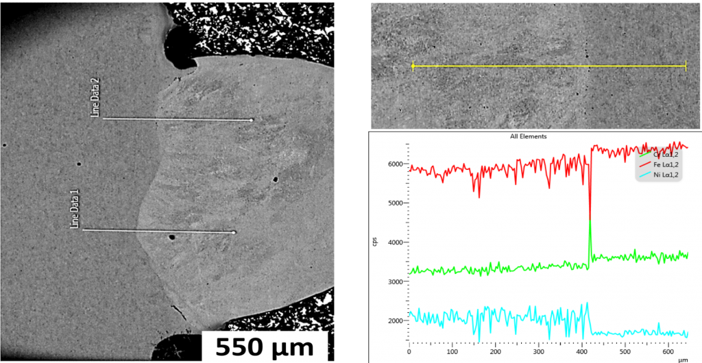
Energy Dispersive X-ray Spectroscopy (EDS)
EDS was used to determine changes in chemical homogeneity. A line-scan was executed across the substrate and printed layer. This EDS line-scan shows the printed layer diffusing into the substrate by the resulting change in chemical composition of Fe and Ni. The Ni content is higher in the print compared to the substrate
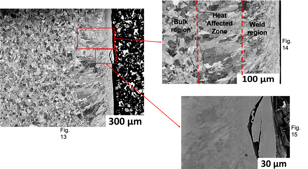
Scanning Electron Microscopy (SEM)
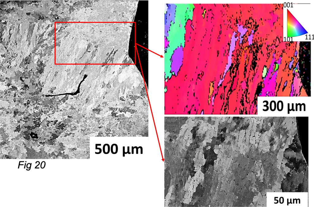
SEM was used to take high resolution, high contrast backscatter electron (BSE) images of all samples. BSE imaging allows for the greatest contrast, showing distinct grain boundaries. The shape and orientation of these grain boundaries shows the direct effect the laser has when compared to the bulk region of the SS substrate, which is elongated grains into the substrate. The laser zone then behaves like a weld region.
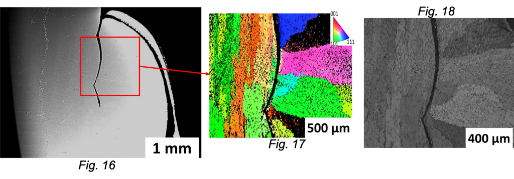
Electron Backscatter Diffraction (EBSD)
EBSD was used to determine the orientation and boundaries of grains in the additive manufactured stainless steel. The AM process using a laser requires the rapid heating and then cooling of a feedstock wire which produces elongated grains. EBSD provided not only a 2-D representation of the grain structure, but the coloration of the image indicates the orientation of the grains in accordance to the inverse pole figure legends.
Conclusions
SEM imaging and EBSD showed the reorientation of grains in the fusion and heat affected zones relative to the bulk microstructure in AM SS. The changes observed in the microstructure may negatively impact the performance and shaping of additive manufactured metals. Generally, grain elongation could be observed in all samples. These findings will aid in a better understanding for the performance of AM alloys in terms of mechanical and corrosion performance testing, and improvements in the additive manufacturing process.
Acknowledgements
- IGEM Award (003612 FY19 IGEM) from Idaho Commerce
- Nick Bulloss – For assistance and training in the use of the electron microscopes and software.
- Phil Boysen – For assistance in use of the band saw and advice for sample sectioning.
Additional Information
For questions or comments about this research, contact Cayden Doyle at caydendoyle@u.boisestate.edu.