

About the Program
The Nanoscale Materials and Device Group has developed an easy-to-use, interactive simulation tool for complex, multi-layer dielectric, MOS and MIM devices. This program is useful for visualizing approximations of energy band diagrams, and performing back-of-the-envelope calculations of their important parameters.
Feature Overview
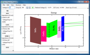
- Draw band diagrams for MOS devices in static mode
- Draw band diagrams for MOS and MIM gate stacks with various dielectrics, including high-κ dielectrics
- Show band diagram movement for MOS and MIM devices as gate voltage is swept through a range
- Calculate these parameters for applied voltages both in inversion and accumulation regimes:
- energy
- electric field
- charge
- potential as a function of distance
- Calculate the following device parameters (and more):
- threshold voltage
- flat band voltage
- equivalent oxide thickness (EOT)
- stack capacitance
- layer capacitance
- tunneling distance
- electric field
- voltage drop
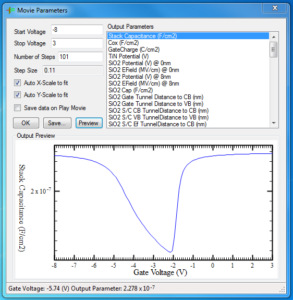
- Plot and export device parameters as a function of gate voltage
- Approximate changes in parameters due to temperature (down to 100 K)
- Insert fixed charge into dielectrics
Example Applications
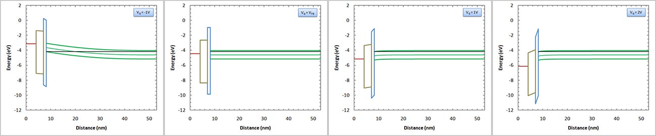
Band Bending With Gate Voltage Shifts
Energy bands can be modeled at varying gate voltages in the program. The following graphs depict a high-κ nMOSFET with the gate bias being swept from -1V to 2V. The program can play a continuous animation of the sweep.
Fixed Charge Insertion
Fixed sheet charges can be placed in any dielectric layer at a user specified distance into the dielectric. Resulting shifts in device parameters and energy levels are easy to observe. Here, a novel dielectric stack for application in nonvolatile memory (NVM) is charged after a ‘write’ operation, and the resulting change in stack capacitance is observed.
Temperature Dependence of Device Parameters
The program can simulate temperature effects on dielectric stacks from 100K to ~600K. A 3.2nm SiO2 nMOSFET was modeled in the program and the threshold and stack capacitance monitored during a temperature sweep.
Comparison of Stack Parameters
By modeling different dielectric stacks, device parameters can be calculated. Demonstrated here is a comparison of three different stacks for possible application to NVM. We compare energy band diagrams (left) and critical stack parameters (right).
Assumptions Used in the Program
In order to draw the diagram and calculate the parameter, many simplifying assumptions have been made and incorporated into the program:
- Ionized dopant temperatures
- Fermi-Dirac approximated with Maxwell-Boltzmann statistics
- Semiconductor doping >> intrinsic carrier concentration
- Complete ionization of dopant atoms
- Non-degeneracy in the semiconductor
- Charge sheet approximation
- Uniformly doped silicon
- Intrinsic Fermi level equals half the bandgap in the semiconductor
- Oxides act as perfect capacitors in series
- Metal gate
Note: Please understand that this program is to be used to gain familiarity of energy band diagrams under bias and is not to meant to replace more accurate models and calculations. Be advised that there are bugs in the program. Relative to both these statements, you should use the program with caution.
Program Download & Tutorial Video
Version 3.1.8 – Rebuilt for Windows 11 and Mac OS Monterey/Ventura
Version 3.1.7 – Rebuilt for Windows 10
Version 3.1.6 – Now compatible with all non-English versions of Windows (Windows 7)
Version 3.1.5 – Added the ability to import materials libraries
Version 3.1.4 – Fixes some issues with graph export
Version 3.1.3 – Java based release
Please send a file download request to Bill Knowlton at bknowlton@boisestate.edu
Energy Band Diagram GitHub Repository
Microsoft Windows Installer (Windows 11 – Version 3.1.8)
File: band3.1.8.exe 59.9 MB
Microsoft Windows Installer (Windows 10 – Version 3.1.7)
File: band3.1.7.exe_.zip 45.7Mb
Microsoft Windows Installer (Windows 7 – Version 3.1.6)
File: band3.1.6.exe.zip 3.4Mb
Mac OS Monterey/Ventura
File: band3.1.8.pkg 59.9Mb
Mac OS X
File: band3.1.6-Mac.zip 3.9Mb
For those with newer Macs, one can obtain Java 6 for OS X Yosemite on the Apple Support Website.
Linux Generic
file: band3.1.6-Generic.zip 3.2Mb
Tutorial Video: Energy Band Diagram
Team
- Richard Southwick (ECE, Summer 2003)
- Aaron Sup (Physics Special Lecturer)
- Dr. Amit Jain (Computer Science)
- Bill Knowlton (ECE & MSE)
- Ryan Thompson (ECE)
- Allen Benz (Computer Science)
References
Primary References
- R.G. Southwick III* and W.B. Knowlton, Stacked Dual Oxide MOS Energy Band Diagram Visual Representation Program, IRW student paper, Invited Paper, IEEE Transactions on Device and Materials Reliability, 6 (2), 136 – 145 (2006). doi: 10.1109/TDMR.2006.876971.
- R.G. Southwick III*, A. Sup, A. Jain, and W.B. Knowlton, An Interactive Simulation Tool For Complex Multilayer Dielectric Devices, IEEE Transactions on Device and Materials Reliability, 11 (2), 236 – 243 (2011). (Note: In IEEE TDMR Top 20 List of Accessed Articles for January 2012). doi: 10.1109/TDMR.2011.2129593.
Additional References
[1] Richard Southwick III, Michael Ogas and William B. Knowlton, Interactive dual oxide MOS energy band diagram program, poster presentation at the 2005 IEEE International Integrated Reliability Workshop, (October 2005).
[2] Aaron Sup, Richard G. Southwick III, Amit Jain, and William B. Knowlton, Arbitrary Oxide Multi-Layer MIM Energy Band Diagram Program, poster presentation at the 2007 IEEE International Integrated Reliability Workshop, (October 15-18, 2007).
[3] Richard Southwick III, Aaron Sup, Amit Jain, and W.B. Knowlton, Multi-Layer Metal-Insulator-Semiconductor (MIS) Energy Band Diagram Program, poster presentation at the 2008 IEEE International Integrated Reliability Workshop, (October 2008).