Imagine shrinking down to the size of an atom and playing a game of catch. A tennis ball is tossed against a wall. At normal proportions, it’s a given that the ball would bounce right back into someone’s waiting hand. But at the atomic level, would that still hold true?
Quantum physics is all about studying the physics that are at play every day of our lives, but at the scale that we can not possibly see with the naked eye: objects measured in nanometers, or one billionth of a meter.
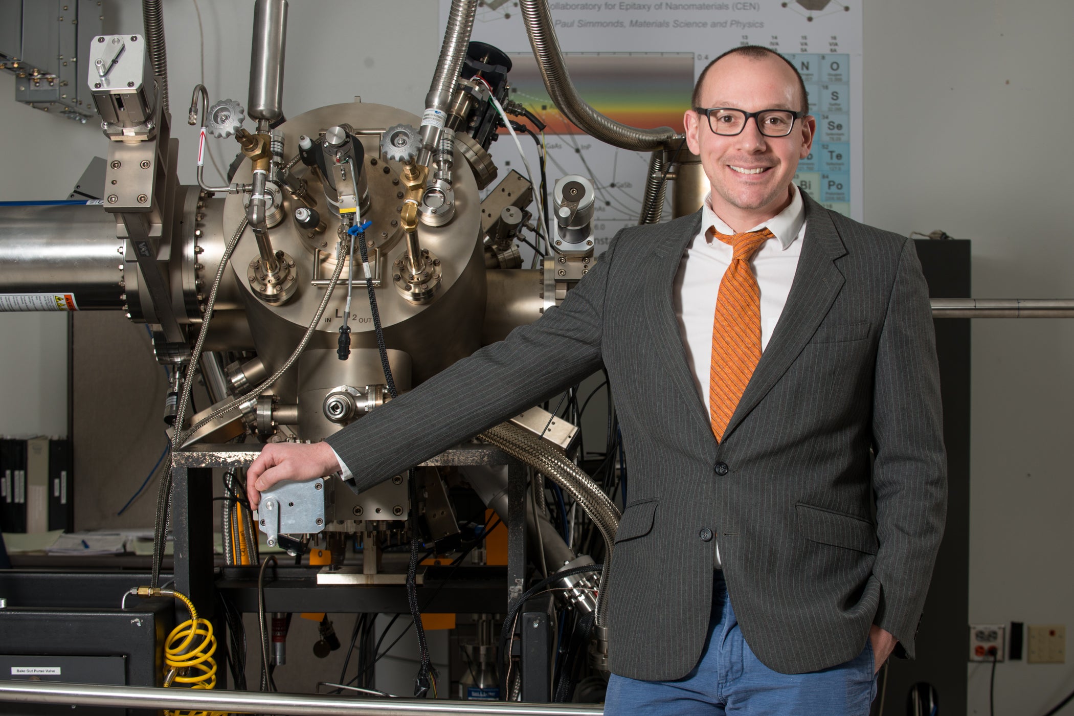
“We can make predictions about the physics that you and I experience in our day-to-day lives very reliably. We know that if we drive our car into a wall, it is not going to end well,” said Paul Simmonds, an assistant professor with a joint appointment in the Department of Physics and the Department of Materials Science and Engineering.
“But it turns out that when you shrink down to length scales approaching that of the atom, then those predictions are no longer correct.”
So that tennis ball thrown at the atomic level? Well, who knows if it’ll come back or not.
For Simmonds, unlocking the mysteries of quantum physics is a chance to create materials whose physical properties and abilities stretch the boundaries of what has been possible until now.
Creating novel nanostructures
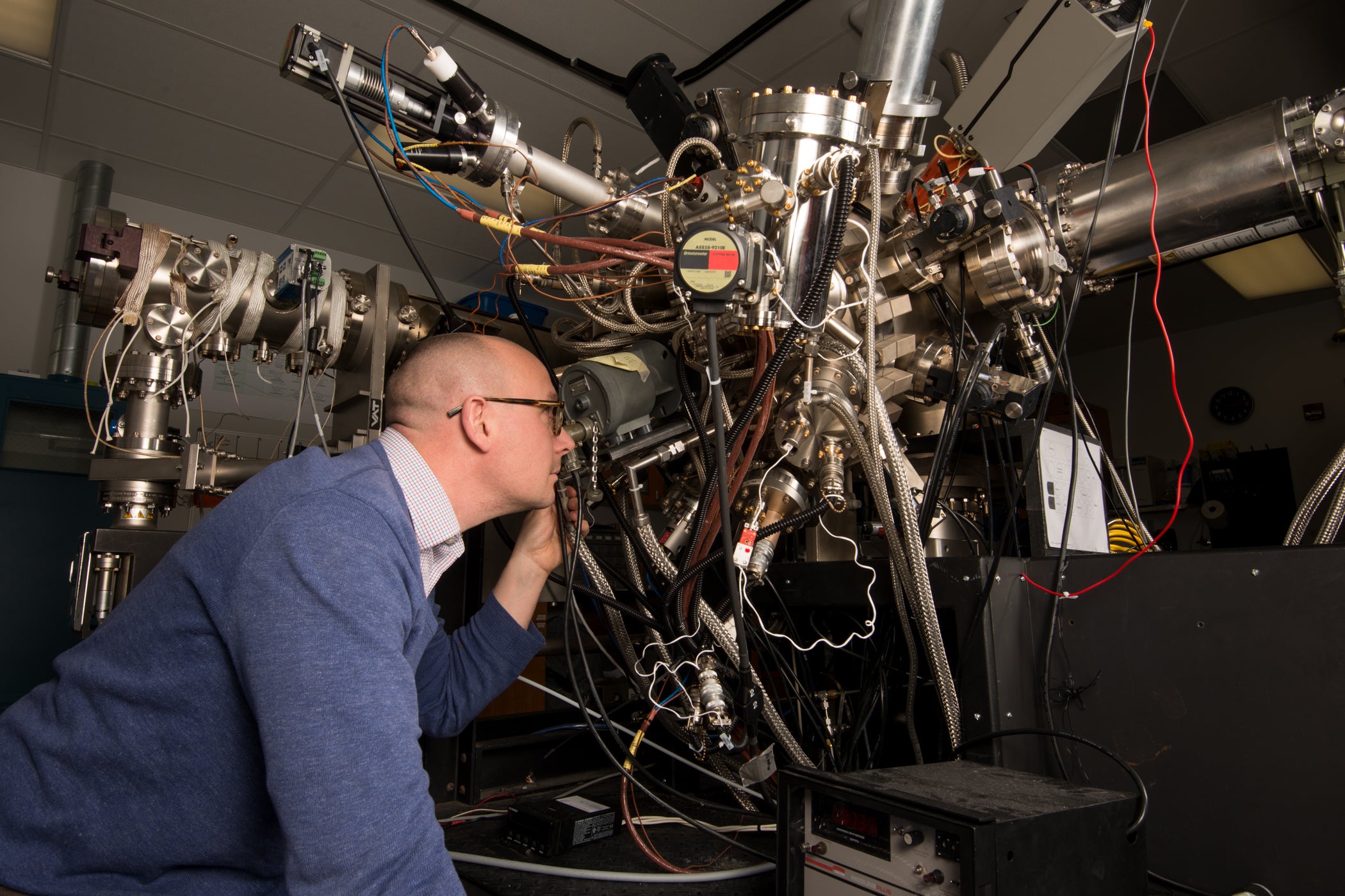
In order to understand how these new materials can be created, it’s helpful to step into the classroom for a quick lesson on molecular beam epitaxy. What this term describes is a process in which beams of atoms or molecules of specific elements are injected into a vacuum chamber and then assemble themselves in a layer on a prepared surface.
To make it even more interesting, the surface that these molecules are assembling on is placed at an unusual angle. This causes the atoms to arrange themselves in a different way than they would on a traditional level surface, and opens up possibilities for them to integrate with different atoms that they normally wouldn’t be able to mesh with.
Simmonds likens the process to rain falling on a waxed car. The raindrops first land on the car in a layer, but as more rain falls, the water forms drops on the surface. In this case, the individual molecular properties of each of the elements control how they assemble. Simmonds calls the drops created through the epitaxy process ’nano droplets’ or ‘quantum dots’, and despite their liquid-like behavior, they are in fact extremely miniscule crystals.
At Boise State, Simmonds leads the Collaboratory for Epitaxy of Nanomaterials, which uses molecular beam epitaxy to grow and design these nanocrystals and new families of nanomaterials with properties for specific applications, such as quantum cryptography and optoelectronics (an area of electronics used in light-emitting or light-detecting devices).
A discovery in the ‘quantum well’
Molecular beam epitaxy has been in use since the 1970s, and has been used in quantum dot development since the 90s. However, when Simmonds discovered a new family of quantum dot nanomaterials, something about them didn’t quite add up.
“During the molecular beam epitaxy process, we can calibrate very precisely how many atoms essentially we are putting down on the surface,” said Simmonds. “If you measure how big these nano droplets are and how many there are per unit area, it doesn’t add up to the number of atoms that we put down on the surface.”
So where were the missing atoms going? Established theory around molecular beam epitaxy could not account for this loss in this new family of nanomaterials. That’s what drove Simmonds to dive into the quantum well to solve the mystery.
Together with his former graduate student Christopher Schuck (Ph.D., materials science and engineering, 2019) who is now at the University of Delaware, Simmonds discovered the answer to the missing atoms in collaboration with researchers from universities in the U.S., China and Mexico. Instead of joining the quantum dots, the missing atoms actually were sinking into the flat surface layer below the dots and making it thicker. This flat layer is called a quantum well and because of the way it connects all of these quantum dots, it may allow the nanocrystals to interact in unexpected ways.
Normally during quantum dot growth, the thickness of this quantum well is fixed, which limits how one could use it. The fact that for these recently discovered quantum dots the quantum well thickness is completely tunable offers greater opportunity for scientists like Simmonds to utilize these nanomaterials for new applications.
“Now, in principle, we could create a situation where we could tune the quantum well and the quantum dots to match each other,” said Simmonds. “And we could get some interesting effects, where we can have really precise control over what the electrons are doing inside these materials, which could have a really powerful impact on electronic devices.”
Examples include infrared optoelectronics and quantum optics applications, which could be used for new types of solar cells with higher efficiency, or future communication systems that are secure against hackers.
Simmonds’ research is supported by National Science Foundation CAREER Grant No. 1555270, for $506,000.
Learn more about Simmonds’ recent discovery
-By Brianne Phillips