Recent research on low-temperature devices and circuits has focused on materials such as organic semiconductors, metal oxides, and chalcogenides. Depending on the specific requirements of the application, different materials may offer advantages. In the case of driver circuits for liquid crystal (LCD) or active matrix organic light emitting diode (AMOLED) displays, transparent semiconducting oxides (TSOs) like IGZO are desirable so that light transmitted to the observer is maximized. But for electronic systems that do not require transparency, silicon has begun to re-emerge as a prime candidate. Although hydrogenated amorphous silicon (a-Si:H) has been extensively investigated in past decades for use in solar cells and thin-film transistors (TFTs), it severely degrades when exposed to light or moderate voltage bias stress. In contrast, nano-crystalline silicon (nc-Si) offers better stability, higher electron mobility, and the ability to conduct holes. A single active layer deposition of nc-Si could potentially produce complementary electronic devices and circuits with high gain and cutoff frequency. Silicon is also an environmentally friendly material, unlike others such as CdS or CdTe.
Nano-crystalline Silicon Material
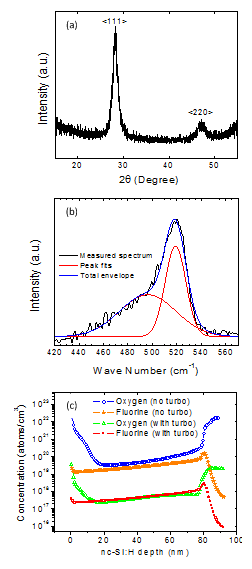
High electron and hole mobility ambipolar nc-Si TFTs have been reported by only three research groups starting in 2006, including our group at UT Dallas. The material is created using plasma-enhanced chemical vapor deposition (PECVD) with SiH4 heavily diluted in pure H2, which helps to induce crystallite formation. A turbomolecular pump is attached to the chamber to achieve base pressure less than 5 µTorr prior to the deposition process. Extensive characterization of these films has been performed. X-ray diffraction (XRD) and Raman spectroscopy were used to determine the grain size of approximately 5 nm and a crystalline volume fraction of approximately 50%, respectively. Secondary ion mass spectroscopy (SIMS) has indicated that the concentrations of oxygen and fluorine were greatly reduced in these films compared to those without the low pressure pumping step. Since oxygen acts as a shallow donor in a-Si:H films, reducing the oxygen content is thought responsible for the ambipolar nature of the nc-Si (its ability to conduct both electrons and holes).
nc-Si TFT Devices
Communication between electronic systems and the brain, involving both invasive and non-invasive interfaces, will be a reality in the future. Brain-computer interfaces can already interact with small numbers of neurons in concentrated areas using electrical probes. However, most signal transmission in the synapses of the brain is chemical, and it is purely electrical interfaces may never provide the correct functionality and precision. Incorporating chemical and biological sensor devices as the interface between the environment and artificial neural networks is possible with low-temperature devices. Similar learning mechanisms to the biological tissue could be implemented, allowing the artificial layers to replace or augment abilities lost due to disease or traumatic brain injury (TBI). In addition to use as a neuroprosthetic that replaces lost functionality, this system could sense depression or other changes in mood, or provide specific information about the operation of the brain. In other words, this interface could essentially provide real-time brain diagnostics, to help determine if sections are malfunctioning or becoming unstable.
TFT Circuits
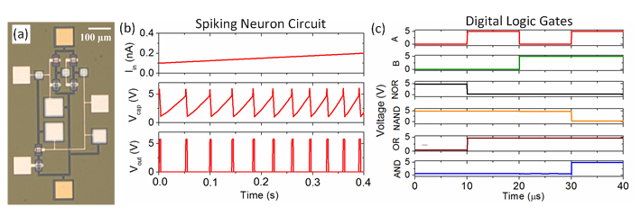
The circuits fabricated with the ambipolar nc-Si TFTs include inverters, buffers, ring oscillators, digital logic gates, and artificial spiking neurons. An optical image of a fabricated Mead neuron circuit is shown above as an example of complex functions that can be implemented using these devices. The operation of this circuit is such that voltage pulses of a few milliseconds duration and constant amplitude are produced upon the injection of current to the input node. A planar capacitor is placed at the input node and the voltage builds up due to the current. Depending on the current magnitude and the amount of current flowing through a leakage TFT biased in subthreshold, the firing rate at the output changes as illustrated in the center plot above. While the neuron circuits are designed to operate at relatively low frequencies (few hundred Hz maximum), many digital and analog circuits will benefit from high cutoff frequencies. Digital logic gates fabricated in the same process run are illustrated at the right, with input A switched at 100 kHz. In addition, inverters switched at 2 MHz showed good performance, but began exhibiting significant delay beyond this point. The primary reason is thought due to the large (~5 µm) gate-to-source/drain overlap, and the subsequent parasitic capacitance. This will be mitigated by the short channel TFTs and more precise lithographical alignment, resulting in drastically increased operation frequency. The overall performance metrics of these ambipolar inverters are generally better than inverters using only n-channel TFTs.