News articles
Active Research Programs
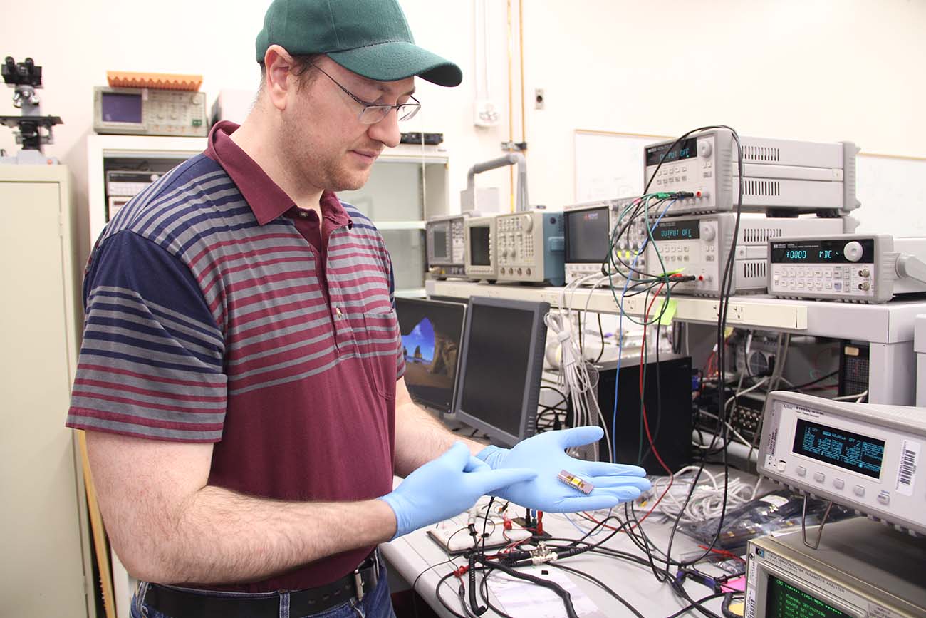
Computer Engineering
Adaptive Hardware and Systems on Reconfigurable Chips
A complete useful adaptive system on FPGA, contains an embedded processor cores along with all other functional hardware components such as memories, input/output and communication interfaces. Adaptation reflects the capability of a system to maintain or improve its performance in the context of internal or external changes such as environmental changes, interference, modification of requirements, trade-offs between performance and resources. In this research, we investigate the use of partial reconfiguration capabilities of FPGAs, and adaptive and evolvable hardware design techniques and platforms in the design and implementation of such systems. These systems are applied to several real world solutions such as: health diagnosis, networks, recognition, identification, inspection, automation, networks, and control.
Neuromorphic Architectures
Neuromorphic architectures have the potential to revolutionize computing efficiency and capability. Drawing inspiration from biology, neuromorphic systems can learn, adapt, and process diverse sets of information originating from a variety of sources. The overall goal is the design of custom hardware solutions to implement various machine learning algorithms. These systems may rely on analog signals, voltage pulses/spikes, or other physical phenomena for information transmission.
MORE INFO
To learn more, visit the Cantley Research Group online.
PARTICIPATING ECE FACULTY
- Kurtis Cantley
FACILITIES
The Electronic and Neuromorphic Device and Systems (ENDS) Lab is located in the Micron Engineering Center, room 312. The Transport Characterization Lab and the Idaho Microfabrication Laboratory are also utlized in this research.
FUNDING
- Defense Threat Reduction Agency contract HDTRA11710036: “Impact of Radiation on Spatio-Temporal Pattern Recognition in Memristor-Based Neuromorphic Circuits”
- National Science Foundation award 1751230: “CAREER: Spiking Neural Circuits and Networks with Temporally Dynamic Learning”
COLLABORATION CAPACITY
This research has opportunities for collaboration in multiple areas of computer science, specifically software machine learning, firmware development, and operating systems
RELEVANT PUBLICATIONS
- R. Ivans and K. D. Cantley, “A Spatiotemporal Pattern Detector,” in 2019 IEEE 62nd International Midwest Symposium on Circuits and Systems (MWSCAS), 2019, pp. 444–447.
- S. G. Dahl, R. C. Ivans, and K. D. Cantley, “Learning Behavior of Memristor-Based Neuromorphic Circuits in the Presence of Radiation,” in Proceedings of the International Conference on Neuromorphic Systems, 2019.
- S. G. Dahl, R. C. Ivans, and K. D. Cantley, “Radiation Effect on Learning Behavior in Memristor-Based Neuromorphic Circuit,” in 2019 IEEE 62nd International Midwest Symposium on Circuits and Systems (MWSCAS), 2019, pp. 53–56.
- S. G. Dahl, R. Ivans, and K. D. Cantley, “Modeling Memristor Radiation Interaction Events and the Effect on Neuromorphic Learning Circuits,” Proc. Int. Conf. Neuromorphic Syst. – ICONS ’18, pp. 1–8, 2018.
- K. D. Cantley, R. C. Ivans, A. Subramaniam, and E. M. Vogel, “Spatio-Temporal Pattern Recognition in Neural Circuits with Memory-Transistor-Driven Memristive Synapses,” in 2017 International Joint Conference on Neural Networks (IJCNN), 2017, pp. 4633–4640.
Sensor Systems
Sensor nodes are composed of small microprocessors connected to a set of sensors and supported by various communications, power management, and data storage systems. Sensor nodes must often be power efficient as they may need to operate for extended periods without external power. The microprocessors used in embedded systems are inherently limited in comparison to the processors inside desktop computers. Embedded processors give up some overall processing power in exchange for both reduced physical size and reduced power requirements. Current research include FAA airliner cabin environmental monitoring and NIH in-home air quality monitoring.
Spiking Neural Networks
This research involves the use of novel semiconductor materials and devices such as memristors for implementing electronic neural networks with biologically realistic behaviors and learning modalities. The motivation for this effort is that the brain is able to process many types of real-world information far more efficiently than today’s digital computers. It is also adept at experiential learning and making predictions and inferences, which are critical properties for future intelligent computers.
MORE INFO
To learn more, contact Kris Campbell (kriscampbell@boisestate.edu) for device research, and Kurtis Cantley (kurtiscantley@boisestate.edu) for circuit research, or visit https://www.boisestate.edu/coen-crg
PARTICIPATING ECE FACULTY
- Kris Campbell
- Kurtis Cantley
FACILITIES
Device fabrication is performed in the Idaho Microfabrication Laboratory. Electrical characterization is performed using state-of-the-art microprobe stations in various labs. More information on electrical characterization can be found on Kris Campbell’s research site.
COLLABORATION CAPACITY
Theoretical neuroscience and cognitive sciences are two potential fields with strong research collaboration potential
FUNDING
- National Science Foundation award 1751230: “CAREER: Spiking Neural Circuits and Networks with Temporally Dynamic Learning”
RELEVANT PUBLICATIONS
- Campbell, K. A.; Drake, K. T.; and Barney Smith, E. H. “Pulse shape and timing dependence on the spike-timing-dependent plasticity response of ion-conducting memristors as synapses,” Frontiers in Bioengineering and Biotechnology (2016) 4, article 97, 1-11. Open access: http://journal.frontiersin.org/article/10.3389/fbioe.2016.00097/full
- R. C. Ivans, S. Member, S. G. Dahl, S. Member, and K. D. Cantley, “A Model for R(t) Elements and R(t)-Based Spike-Timing-Dependent Plasticity With Basic Circuit Examples,” IEEE Trans. Neural Networks Learn. Syst., vol. PP, pp. 1–11, 2019.
- R. C. Ivans, K. D. Cantley, and J. L. Shumaker, “A CMOS Synapse Design Implementing Tunable Asymmetric Spike Timing-Dependent Plasticity,” in International Midwest Symposium on Circuits and Systems (MWSCAS), 2017, pp. 0–3.
Wireless Sensor Networks
Frequently, individual sensor nodes are connected wirelessly to form wireless sensor networks. Networking sensor nodes allows scientists to more accurately characterize phenomenon of interest by providing a means to both temporally and spatially relate sensor data.
Integrated Circuit Design
Analog to Digital Converter (ADC) Design
Boise State’s Mixed Signal IC design group has active research program in development of High-Speed Continuous-time Delta-Sigma Analog-to-Digital Converters (ADCs) and novel reconfigurable and hybrid-ADC architectures. The ADCs are targeted towards next-generation wireless communication systems and software-defined radios (SDRs).
High-speed Interconnects
Research in this area involves developing energy-efficient >10 Gb/s serial links for electrical as wells as optical interconnects. The research involves circuit design for transmitters, receivers, equalizers and clock data recovery (CDR) and PLLs. Integrated CMOS photonics circuit design for next-generation interconnects and on-chip IOs is the primary focus of this research thrust.
Neural Interfaces
We are interested in developing novel electrodes and circuits that improve our ability to record and modulate neural activity. Neural interfaces are a critical component for studying the function of neural circuits or building therapeutic devices to treat neurological dysfunction. Advanced materials and microfabricated structures can reduce the damage caused by neural implants, increase electrical stimulation capacity, and improve the signal-to-noise ratio of recorded signals. Optimized integrated circuits for neural interfaces can improve the battery life of implanted devices and achieve complex system integration in a vanishingly small form factor.
MORE INFO
To learn more, visit the researchers’ websites:
PARTICIPATING ECE FACULTY
- Kurtis Cantley
- Ben Johnson
FACILITIES
The Electronic and Neuromorphic Device and Systems (ENDS) Lab is housed in the Micron Engineering Center, room 312. This research also utilizes the Transport Characterization Lab in the Ruch Engineering Building, room 109.
FUNDING
- INBRE-4 DRP: Strategies to Mitigate Fibrous Encapsulation of Neural Implants
COLLABORATION CAPACITY
This research has numerous opportunities for collaboration in theoretical and experimental neuroscience, neurosurgery, and neurology
RELEVANT PUBLICATIONS
- S. Rastegar, J. Stadlbauer, T. Pandhi, L. Karriem, and K. Fujimoto, “Measurement of Signal-to-Noise Ratio In Graphene-based Passive Microelectrode Arrays,” Electroanalysis, 2019.
- S. Rastegar, J. Stadlbauer, K. Fujimoto, K. Mclaughlin, D. Estrada, and K. D. Cantley, “Signal-to-Noise Ratio Enhancement Using Graphene-Based Passive Microelectrode Arrays,” in International Midwest Symposium on Circuits and Systems (MWSCAS), 2017.
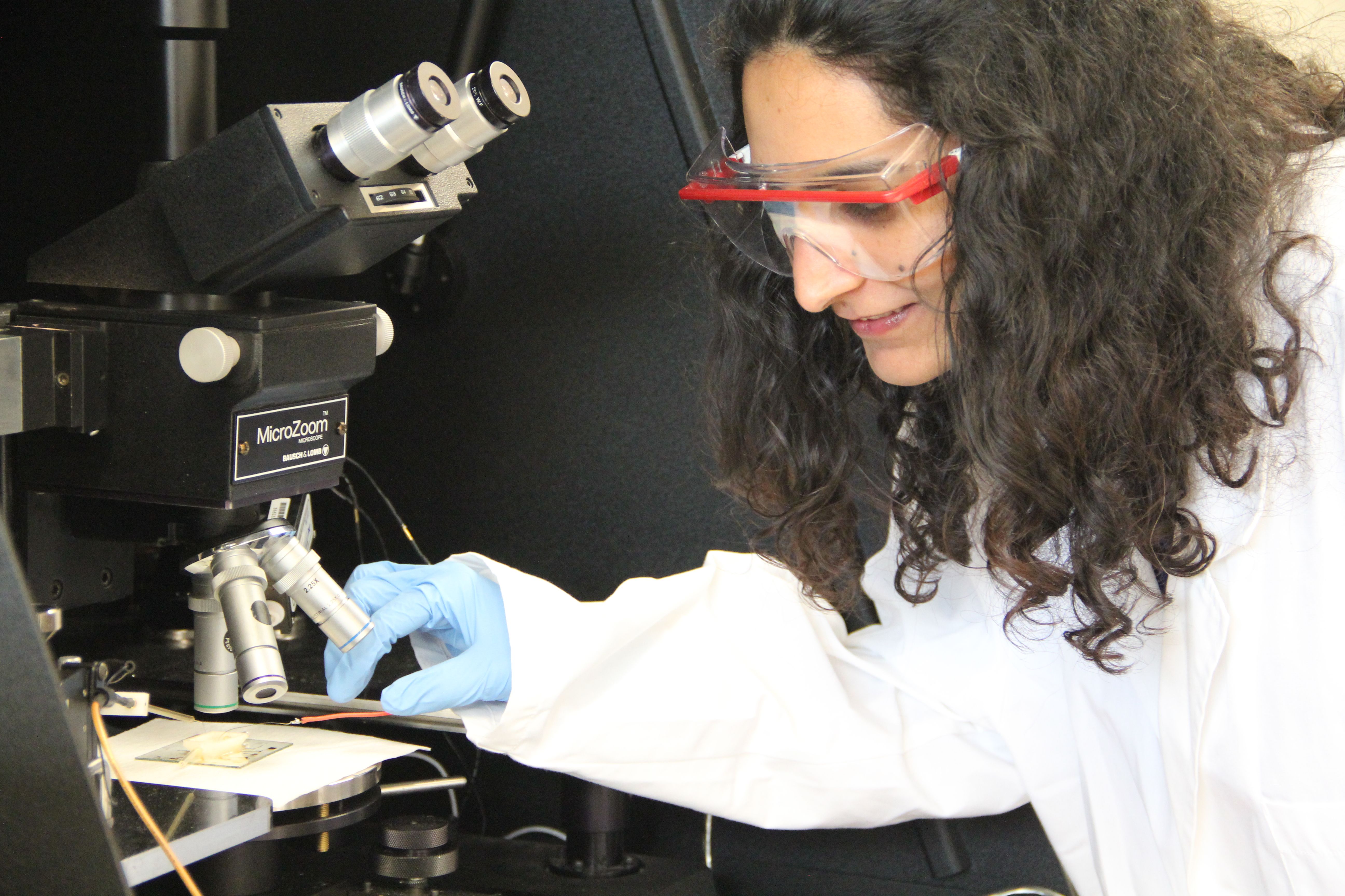
Nanoscale Electron Devices
Memristor Device Design and Fabrication
We develop novel memristor device technologies to foster improved development of neuromorphic computing technologies and for novel applications. This includes device materials, structures, and nanofabrication methods.
This technology allows researchers to explore applications ranging from robotic control to neuromorphic computing.
MORE INFO
To learn more, visit the Electronics and Natural Sciences Research Lab online.
PARTICIPATING ECE FACULTY
- Kris Campbell
OTHER COLLABORATORS
- Knowm, Inc. (Knowm.org)
FACILITIES
Device fabrication is performed in the Idaho Microfabrication Laboratory. Electrical characterization is performed using state-of-the-art microprobe stations. More information on electrical characterization can be found on Kris Campbell’s research site.
RELEVANT PUBLICATIONS
- Drake, K., Lu, T., Majumdar, M.H.K., & Campbell, K.A. (2019) Comparison of the Electrical Response of Cu and Ag Ion-Conducting SDC Memristors Over the Temperature Range 6 K to 300 K. Micromachines 10 (10), 663. https://www.mdpi.com/2072-666X/10/10/663/htm
- Campbell, K.A. The Self-directed Channel Memristor: Operational Dependence on the Metal-Chalcogenide Layer. In Handbook of Memristor Networks (2019). Eds. Chua, L., Sirakoulis, G. Ch., Adamatzky, A., 815-842, Springer, Chennai, India.
- Campbell, K. A. (2017). Self-directed channel memristor for high-temperature operation. Microelectron. J., 59, 10–14. https://www.sciencedirect.com/science/article/pii/S0026269216303779
- Campbell, K. A.; Drake, K. T.; and Barney Smith, E. H. (2016) Pulse shape and timing dependence on the spike-timing-dependent plasticity response of ion-conducting memristors as synapses. Frontiers in Bioengineering and Biotechnology (2016) 4, article 97, 1-11. Open access: http://journal.frontiersin.org/article/10.3389/fbioe.2016.00097/full
Nano Devices and Materials
The Nano research group explores novel materials and the electrical properties of devices fabricated with those materials. These materials include chalcogenide-based materials used as memristors, as non-volatile memory, and in reconfigurable electronics applications.Materials studied are fabricated or deposited within our group or with other university or industry collaborators. We have several materials characterization instruments in our laboratory, including a microRaman spectrometer, modulated differential scanning calorimeter, n&k tool for film optical properties, atomic force microscope, and a continuous-wave electron spin resonance spectrometer equipped with a dual-mode cavity. For device characterization, we have 4 microprobe stations, two of which are capable of variable temperature operation between 4.2 K to 400 K. We use the Idaho Microfabrication Laboratory (IML) to process devices. In addition, we regularly integrate our materials into the back-end-of-line CMOS processes.
Nanoionic Materials and Devices
The research work carried out by the Nanoionic Materials and Devices group is mainly related to characterization of the structure of chalcogenide glasses doped with Ag or Cu, as well as formation and testing of conductive bridge memristors and arrays based on them. Further aspect of the research work is related to creation of radiation sensors utilizing the radiation sensitivity of chalcogenide glasses (ChG) and radiation induced ions diffusion in them which results in drastic conductivity change.
Optically Gated Transistors
The Campbell Research group has developed an optically gated transistor (OGT) device that exhibits IV curves similar to a metal oxide semiconductor field-effect transistor (MOSFET). In the OGT, there are only two electrical terminals, a source, and a drain. The MOSFET equivalent gate terminal of the OGT is not an electrode, but instead is simply an optically sensitive material that allows current flow between the source and drains electrodes when illuminated. In this way, light on the material performs the same function as voltage on the gate electrode of a MOSFET. We are exploring materials modifications to the OGT that enable tuning of the transistor properties, such as maximum saturation current, and light wavelength response. The operational physics of the device is also a research area under study.
The OGT has been demonstrated for use as a selector for a memristor device where it is used to gate access to the memristor and to allow continuous programming of the memristor state via intensity of incident light.
MORE INFO
- Contact Kris Campbell (kriscampbell@boisestate.edu)
PARTICIPATING ECE FACULTY
- Kris Campbell
OTHER COLLABORATORS
- Knowm, Inc.
- Pearlhill Technologies, LLC.
FACILITIES
Device fabrication is performed in the Idaho Microfabrication Laboratory. Electrical characterization is performed using state-of-the-art microprobe stations. More information on electrical characterization can be found on Kris Campbell’s research site.
RELEVANT PUBLICATIONS
- An Optically Gated Transistor Composed of Amorphous M + Ge2Se3 (M = Cu or Sn) for Accessing and Continuously Programming a Memristor. Kristy A. Campbell, Randall A. Bassine, Md. Faisal Kabir, and Jeremy Astle. ACS Applied Electronic Materials 2019 1 (1), 96-104
DOI: 10.1021/acsaelm.8b00034
Quantum Bit Design
This research investigates materials and device structures with the goal of achieving a room temperature stable quantum memory bit. A limitation of quantum computing is the instability of the state above cryogenic temperatures. We are investigating materials that exhibit spin-spin coupling leading to zero-field splitting as the mechanism of operation. These materials include biological proteins and inorganic model complexes.
MORE INFO
To learn more, contact Kris Campbell (kriscampbell@boisestate.edu).
PARTICIPATING ECE FACULTY
- Kris Campbell
OTHER COLLABORATORS
- US Department of Defense
FACILITIES
Device fabrication is performed in the Idaho Microfabrication Laboratory. Electrical characterization is performed using state-of-the-art microprobe stations. More information on electrical characterization can be found on Kris Campbell’s research site.
Neuromorphic Computing
Neuromorphic Architectures
Another team of investigators is exploring the integration of memristor arrays with CMOS transistor structures to implement a bio-inspired or neuromorphic design, where the memristors simulate synapses (weights), and CMOS structures form the neural soma or summing nodes. This new architecture constitutes a basis of an adaptive bio-inspired processor which has applications in a variety of fields.
Neural Systems and Interfaces
This research area aims to combine the unique properties and capabilities of neuromorphic architectures with nanoscale systems that interface directly with the environment. Creating mechanically flexible circuits that can conform to many different surface topologies including that of biological tissue is a particular focus. Examples include arrays of pressure and thermally sensitive devices for an artificial robotic skin, chemical sensor arrays (artificial olfaction), and electrode arrays for neural interfaces.
Photonics
Integrated Silicon Photonics
Integrated silicon photonics is an emerging area of research and development and is considered the enabler of yet higher data rates for next-generation computing, ‘green’ energy-efficient data centers and biomedical sensing. The research involves high-speed circuit design which combines the high optical bandwidth silicon photonics with the well-established CMOS signal-processing paradigms, all on the same chip.
Optical Devices and Nanophotonics
The mission of nanophotonics research is to scale optical devices and components to their ultimate size limits. This usually involves designing near-field optical interactions that guide electromagnetic energy on a scale well below the diffraction limit.
Plasma Engineering
Cold Plasma for Medicine, Agriculture, and Space
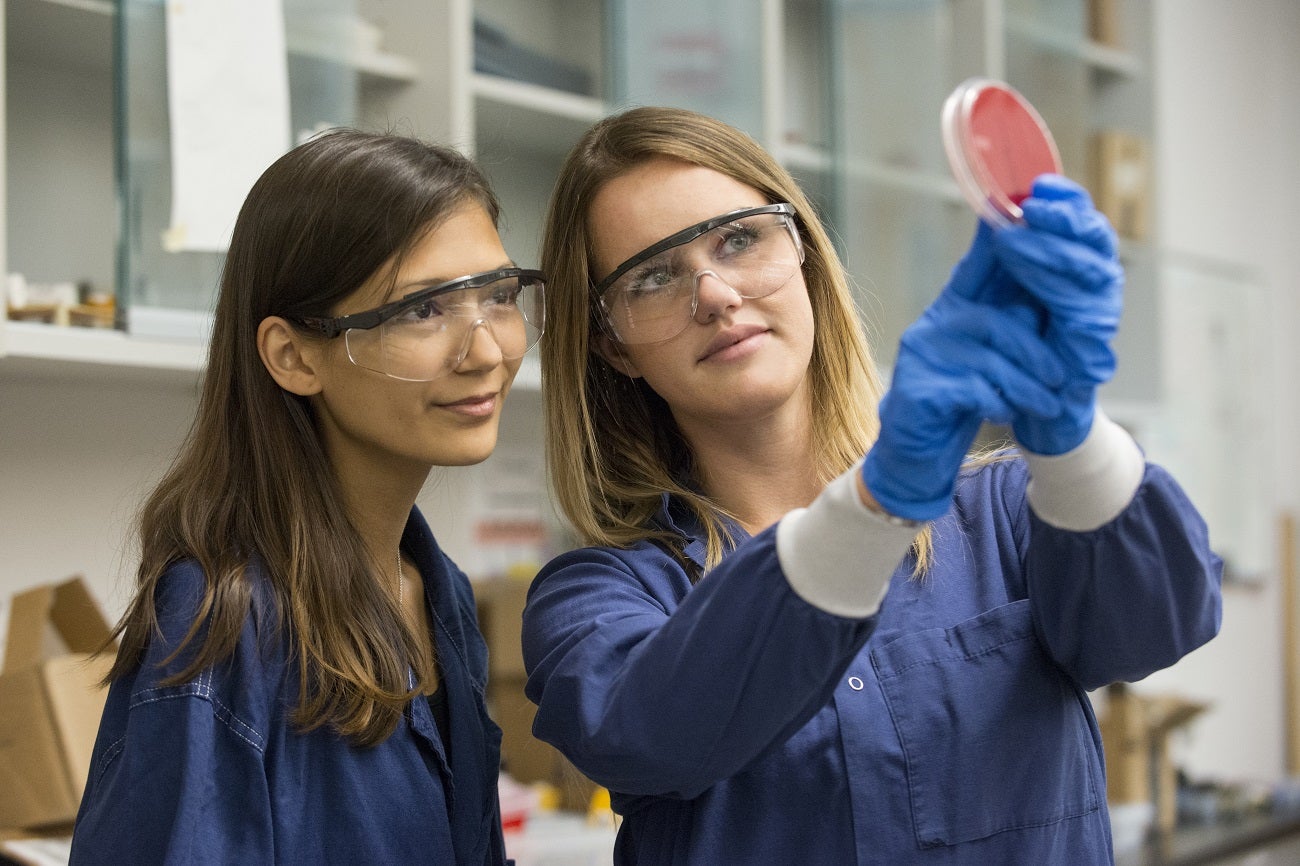
Our research involves the use of cold atmospheric pressure plasma to kill bacteria and biofilms in chronic wounds and on surfaces used in food processing. It also involves utilizing plasma for in-space applications such as sterilization and plasma-assisted printing. The plasma sources can be fabricated in large arrays or in narrow scalpels to either remove biofilm over large areas or selectively remove biofilm from wounds without hurting healthy tissue. This work is primarily experimental and highly transdisciplinary.
Biofilms in food processing cause millions of illnesses a year and require the use of harsh chemicals and large quantities of water. The plasma could reduce the incidence of illness and reduce the need for chemicals and water. The plasma scalpel could improve healing when used to debride chronic wounds, a major health issue for diabetic patients in particular. In-space utilization would also require methods to sterilize surfaces or treat eating utensils to minimize the use of chemicals in space. Plasmas can also be used to aid in aerosol jet printing to improve adhesion for in-space manufacturing.
MORE INFO
To learn more, see Jim Browning’s research page.
PARTICIPATING ECE FACULTY
- Jim Browning
- Nirmala Kandadai
- Harish Subarraman
OTHER COLLABORATORS
- Ken Cornell, Professor of Biochemistry at Boise State University
- Don Plumlee, Associate Professor of Mechanical and Biomedical Engineering at Boise State University
- Julie Oxford, Professor of Biology at Boise State University
- Sam Minnich, Professor of Food Science at the University of Idaho
FACILITIES
Laboratory facilities include two different cold plasma apparatus for studying the effects of plasma on biofilms. A third apparatus is available in Ken Cornell’s lab for research on pathogenic bacteria. The systems are used to study the effects of single plasma devices (plasma scalpel) as well as plasma arrays. One system allows movement of the treatment substrate to and imaging of the substrate for dynamic control of the plasma treatment.
FUNDING
- National Aeronautics and Space Administration
- National Institutes of Health
- United States Department of Agriculture
COLLABORATION CAPACITY
The plasma medicine and agriculture research group has the capacity to collaborate on simulation and experimental work related to plasma diagnostics and plasma generation systems. We’re looking for expertise in image analysis, plasma theory/experimentation, food microbiology, and food processing.
Power and Energy Systems
Advanced FPGA Implementation of Electric Machine Drives
High-performance electric drives necessitate modern and sophisticated controllers involving fast and extensive computations. FPGAs are widely used in this area of research to emulate different control methodologies and their design verification. In the case of induction machines, various control methodologies such as sensorless Direct Torque Control (DTC), Neural Network (NN) Control and Fuzzy Logic (FL) Control can be implemented and tested on FPGA chips. Current research aims at creating a hybrid FPGA/embedded-microprocessor platform for the rapid prototyping of new control algorithms for the purpose of improving cost, speed, and performance of induction machine drives.
Signal Processing
Audio Signal Processing
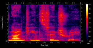
The initial research focus will be on audio source separation of individual string contributions in guitar audio, which has applications to tablature transcription, fixing audio with mistuned strings, and conversion of pitches to just intonation (something that is not physically possible to play directly on a fretted instrument). If the last of these applications can be accomplished in real-time it could be turned into an interesting commercial product in the form of a guitar “pedal”. Audio signal processing can be used in systems that help the aurally impaired.
Students transform and analyze audio signals with Python toolkits, become familiar with professional-grade audio recording equipment, and be able to apply basic music theory to the analysis of music audio. Future research is expected to involve other types of audio signals.
MORE INFO
Read about the Vertically Integrated Project in Audio Signal Processing
PARTICIPATING ECE FACULTY
- Jennifer Smith
FACILITIES
Equipment used in this research project resides in the Signal Processing Lab, housed in the Micron Engineering Center, room 202P.
- Signal Processing Lab (MEC 202P)
- MacBook Pro with Logic Pro X audio editing software
- Two-input Scarlett 2i2 audio interface
- Shure SM58 and Sennheiser 835 microphones
- XLR and instrument cables; mic stands
- Audio processing using Python and librosa audio processing library
COLLABORATION CAPACITY
Interested to collaborate on projects involving voice, music, or other audio as well as the detection of audio “deep fakes” voice audio.
Automatic Music Transcription
Research featuring the automatic tablature transcription of acoustic guitar audio recordings has commercial applications. It is hoped that the transcripts produced can aid in the decomposition of recordings into six individual-string audio files. This would allow the correction of a mistuned string followed by the recombination of audio. It would also allow conversion of the audio to a just intonation tuning from equal temperament. Just intonation is the preferred tuning and can be accomplished with fretless instruments such as violin, but is not practically achievable for fretted instruments such as the guitar.
MORE INFO
To learn more, read about the Vertically Integrated Project in Audio Signal Processing.
PARTICIPATING ECE FACULTY
- Jennifer Smith
OTHER COLLABORATORS
- Justin Stadlbauer, ECE graduate student
FACILITIES
Equipment used in this research project resides in the Signal Processing Lab, housed in the Micron Engineering Center, room 202P.
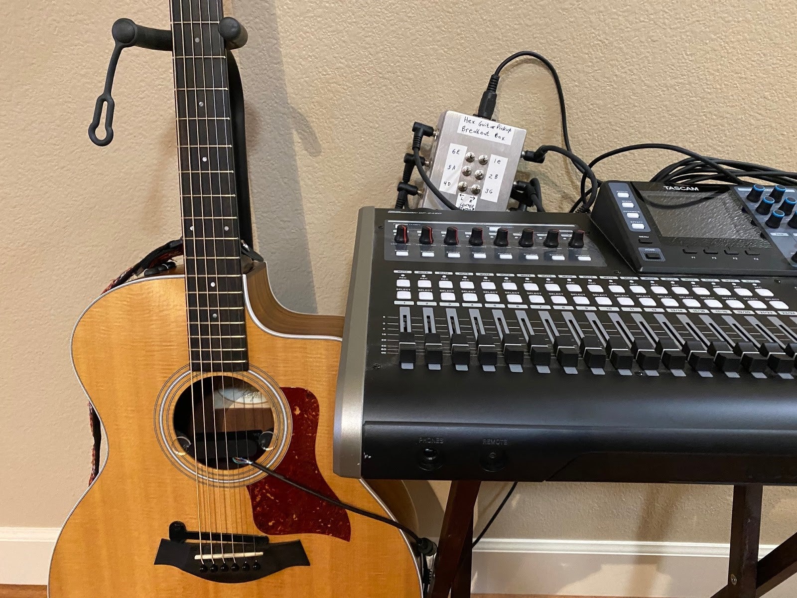
- Taylor 214ce and Fender DG8 acoustic guitars
- Hex guitar pickup (individual string audio breakout)
- TASCAM DP-24SD 8-channel simultaneous audio recording
- MacBook Pro with Logic Pro X audio editing software and Sibelius music engraving software
- Two-input Scarlett 2i2 audio interface
- Shure SM58 and Sennheiser 835 microphones
- XLR and instrument cables; mic stands
- Audio processing using Python and librosa audio processing library
COLLABORATION CAPACITY
Jennifer is a music performer and songwriter who has studied at Berklee College of Music. She is familiar with professional music recording and production as well as music theory and composition.
Noise Enhanced Signal Processing (NESP)
Realizing the fact that almost all the systems are suboptimal in certain ways, NESP provides a low-cost and adaptive ways to improve system performance. Instead of redesign and re-implement of new systems, NESP improves the system performance by changing the input to the system via injecting NOISE. Research in this area involves design and develop novel NESP algorithms for emerging applications and exploration of the performance limit of the NESP approaches.
Vacuum Electron Devices
Microwave Vacuum Electron Devices
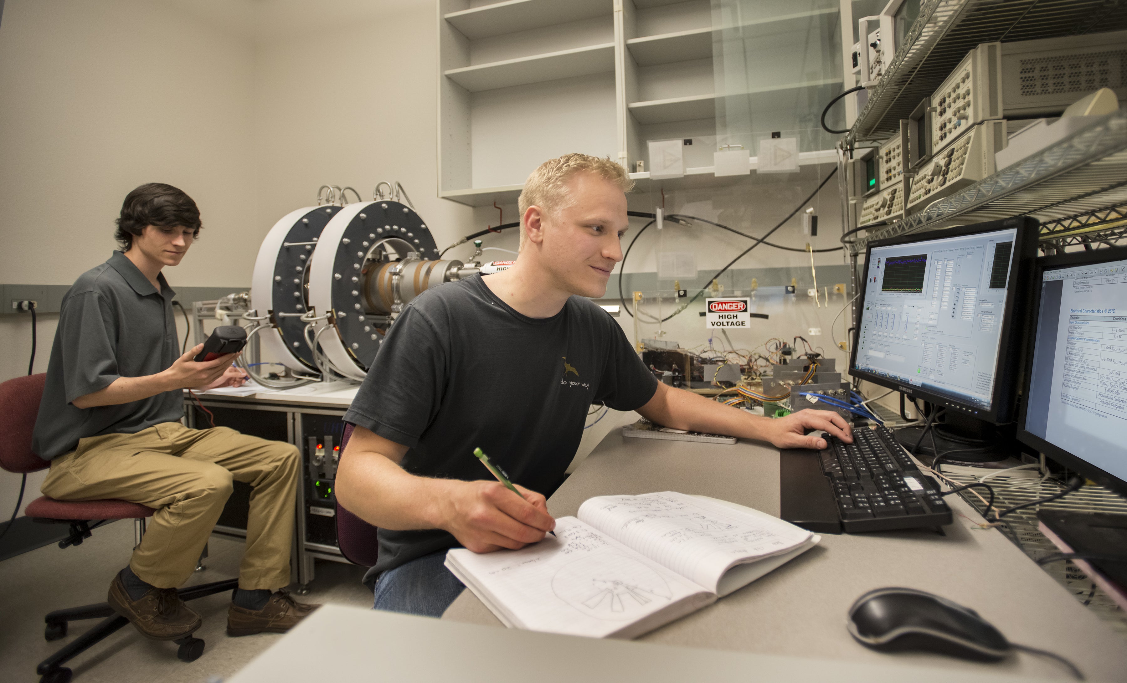
The Browning Research Group focuses on the experimental and simulation study of crossed-field microwave devices including magnetrons and crossed-field amplifiers. Their research looks at the fundamental aspects of electron hub perturbations on device stability and noise and on the use of electron modulation using gated field emission arrays to control the device performance. Improvements in startup time, noise, jitters, gain, and phase control are studied.
The microwave vacuum electron devices include microwave sources (oscillators) and amplifiers used in industrial, civilian, and military applications. Current research focuses on using microwave devices to improve their performance in terms of efficiency, gain, and phase-control.
MORE INFO
To learn more, see Jim Browning’s research page.
PARTICIPATING ECE FACULTY
Jim Browning
OTHER COLLABORATORS
- Tayo Akinwande, Professor in Electrical Engineering and Computer Science, Massachusetts Institute of Technology
- Allen Garner, Associate Professor, Nuclear Engineering, Purdue University
- Don Plumlee, Associate Professor of Mechanical and Biomedical Engineering at Boise State University
- Mike Worthing, Electron Device Division, L3-Harris Technologies
FACILITIES
The Vacuum Electron Devices Laboratory focuses on all aspects necessary to develop, test, and improve the operation of microwave vacuum electron devices. Capabilities include a vacuum array test chamber to characterize electron source, a crossed-field device physics chamber to study the effects of perturbations on electron stability, and a magnetron test chamber to study the effects of electron modulation on magnetron behavior. This research also includes the use of the simulation VBsim and CST.
FUNDING
Air Force Office of Scientific Research
COLLABORATION CAPACITY
Experience in vacuum electron devices and the areas related to electromagnetics create the capacity to work on a range of problems associated with the design, simulation, and fabrication of microwave sources and amplifiers. Experimentally this includes an understanding of vacuum systems, network analyzers, spectrum analyzers, data acquisition and control, and a range of HV and high current power supplies. Our group is looking for expertise in vacuum electron device theory and simulation, microwave systems experimental work, and RF circuit design.
RELEVANT PUBLICATIONS
- Marcus Pearlman and Jim Browning, “Simulation of a Time-Varying Distributed Cathode in a Linear Format Crossed-Field Amplifier,” IEEE Trans. Plasma Science, Vol 47, pp. 3960-3966 (2019); DOI: 10.1109/TPS.2019.2924376
- S Fernandez-Gutierrez, J Browning, MC Lin, DN Smithe, J Watrous, “Dynamic phase-control of a rising sun magnetron using modulated and continuous current,” J. Appl. Phys., Vol. 119, 044501 (2016). doi.org/10.1109/TPS.2018.2844732
- J. Browning and J. Watrous, “A faceted magnetron concept using field emission cathodes,” J. Vacuum Science and Technology B, Vol. 29, March/April (2011).
Vacuum Nano-Transistors
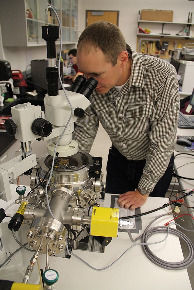
Research into vacuum nano-transistors (VNTs) involves the study and characterization of micro-fabricated transistors. These transistors operate in a vacuum and are resilient in high-temperature (500C) and high-radiation environments. Current research includes:
- characterization of transistor performance in different ambients
- study of device reliability and failure mechanisms
- study of device lifetime and the causes of degradation
- simulation of device performance
Vacuum nano-transistors can be used for space applications to reduce or eliminate susceptibility to radiation (e.g., solar flares) and are possible solutions for nuclear applications including for in-reactor sensors and electronics. They are also useful in a range of high temperature environments.
MORE INFO
To learn more, see Jim Browning’s research page.
PARTICIPATING ECE FACULTY
Jim Browning
OTHER COLLABORATORS
- Tayo Akinwande, Professor of Electrical Engineering and Computer Science at MIT
- Karl Berggren, Professor of Electrical Engineering and Computer Science at MIT
- John Cary, Professor of Physics, University of Colorado
- Luca Daniels, Professor of Electrical Engineering and Computer Science at MIT
- Bruce Gnade, Clinical Professor of Mechanical Engineering at Southern Methodist University
- Tomas Palacios, Professor of Electrical Engineering and Computer Science at MIT
FACILITIES
The Vacuum Electron Devices Laboratory has two major experimental systems for the test, characterization, and failure analysis of vacuum nano-transistors. A characterization chamber system uses a micromanipulator to allow probing of a wide variety of VNTs. The system has a heater chuck capable of testing parts up to 400C. A second lifetime system allows testing of devices for hundreds to thousands of hours while monitoring transistor performance and looking for failures of the structures. Simulations using CST and VSim support this experimental research.
FUNDING
Air Force Office of Scientific Research
COLLABORATION CAPACITY
Experience in vacuum electron devices and the areas related to electromagnetics create the capacity to work on a range of problems associated with the design, simulation, and fabrication of vacuum electron devices including VNTs. Our group is looking for expertise in vacuum electron devices, VNT characterization, and simulation.