Jasen Nielsen
Undergraduate Research Assistant
Department of Mechanical & Biomedical Engineering
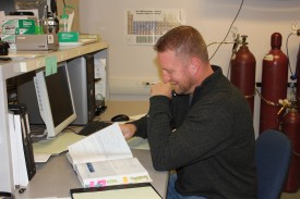
Jasen joined the Nanoscale Materials and Device Group in June of 2012 at the conclusion of his freshman year at BSU. Since then he has worked in the Surface Science Lab, helping NMDG members and other groups advance their research using atomic force microscopy (AFM), associated surface probe microscopy (SPM) techniques, and scanning electron microscopy (SEM). Jasen is a nontraditional student majoring in mechanical engineering, having already earned a B.S. in business management from the University of Phoenix (2005). He has an extensive mechanical background that includes serving as a mechanic on a nuclear submarine, working as an industrial mechanic for a large manufacturing facility, and overseeing residential and commercial construction and project management.
During his time at Boise State, Jasen has been the recipient of both a National Science Foundation (NSF) scholarship and a competitive internship with the US Navy at their Puget Sound Naval Shipyard (PSNS). He was also a finalist for the national SMART scholarship awarded by the Department of Defense (DOD). Upon graduation, he has a position lined up at PSNS in Bremerton, WA, to help create new technologies designed to protect those that serve in the armed forces defending the American way of life. Jasen is an expert user on all of the Surface Science Lab’s AFMs, and enjoys training new students, assisting existing users, and carrying out independent projects to further the research programs of SSL collaborators. Two of the many projects Jasen has helped lead include investigating the effect of ion bombardment on the nanomechanical properties of ferritic/martensitic steels with members of Professor Janelle Wharry‘s group (Boise State Materials Science & Engineering) and characterizing a novel chalcogenide-based nonvolatile memory device developed by Professor Maria Mitkova‘s group (Boise State Electrical & Computer Engineering) as a function of applied bias voltage. The former project is of interest to the nuclear power industry, which would like to use such steels for next-generation power plants, while the latter enabled switching and imaging of the memory device in both logical memory states. Both were quite challenging to accomplish, but resulted in important insights.
Instruments and Techniques
- Atomic Force and Surface Probe Microscopy (AFM/SPM)
- Topography and Surface Roughness Analysis
- Contact
- Noncontact
- PeakForce
- Tapping
- Electrical Characterization
- Conductive and Tunneling AFM (CAFM/TUNA)
- Electric and Kelvin Probe Force Microscopy (EFM/KPFM)
- Fluid Imaging
- Magnetic Force Microscopy (MFM)
- Nanomechanical Properties Measurement
- Nanoindentation
- Quantitative Nanomechanical Mapping (QNM)
- Topography and Surface Roughness Analysis
- Scanning Electron Microscopy (SEM)
Publications
Peer Reviewed Journal Publications
Coming soon.
Conference Presentations and Posters
Wharry, J. P., Dolph, C. K., Hosemann, P., Nielsen, J. & Davis, P. H. “Irradiation-induced microstructure and mechanical property evolution in an Fe-9Cr ODS alloy” presented at 8th International Conference on Processing & Manufacturing of Advanced Materials (THERMEC), Las Vegas, NV (December 2013).