Oleksandr Novyskyy, Dr. Ranajoy Bhattacharya, Jessica Carlson, Adam Croteau, Addie Higgins, John McClarin, David Vogel, Dr. Jim Browning
This research is focused on the development and characterization of transistor devices that use Ultra-High Vacuum (< 10-7 Torr) as the channel for current to flow from the emitter to the collector. Devices are fabricated outside of Boise State University and tested here to determine output current – input voltage (IV) characteristics and performance under high temperatures of 400 °C and tested until failure to determine lifetime. The ultimate goal of the research is to develop a device that is capable of operating inside of a nuclear reactor. The theory and prior research behind nanoscale vacuum channel transistors shows that they are much more resistant to radiation and high temperatures than a typical modern silicon semiconductor device.
Introduction
The goal of Nano Channel Vacuum Transistor (NVCT) research is to develop and characterize three-terminal vacuum transistor devices that operate in ultra-high vacuum (UHV) and withstand temperatures up to 400 °C. This process includes designing driver systems, implementing automated Data Acquisition (DAQ) hardware, and using data to determine approximate lifetime, maximum operating conditions, and identify causes of device failure.
Experimental Setup
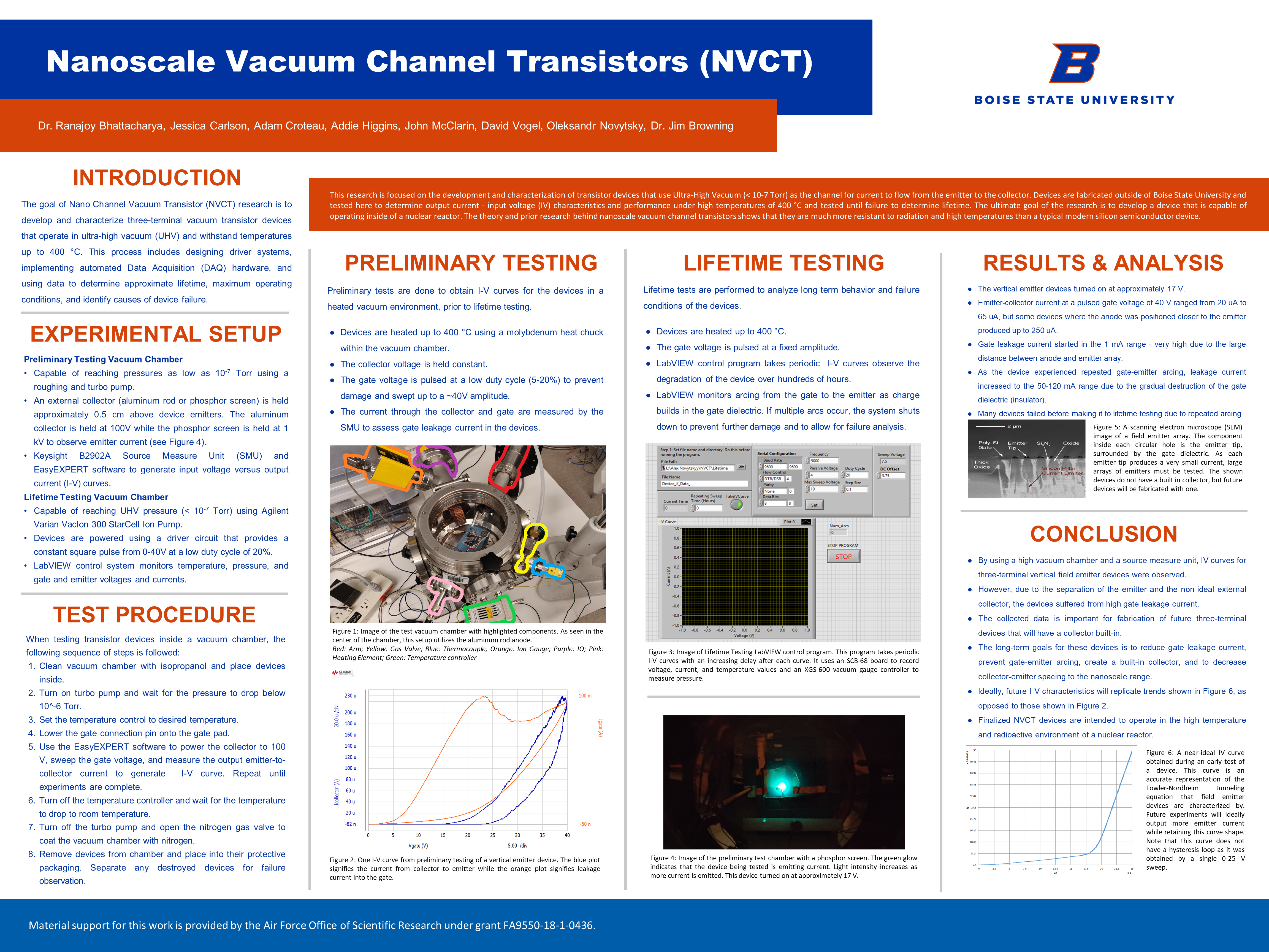
Preliminary Testing Vacuum Chamber
- Capable of reaching pressures as low as 10-7 Torr using a roughing and turbo pump.
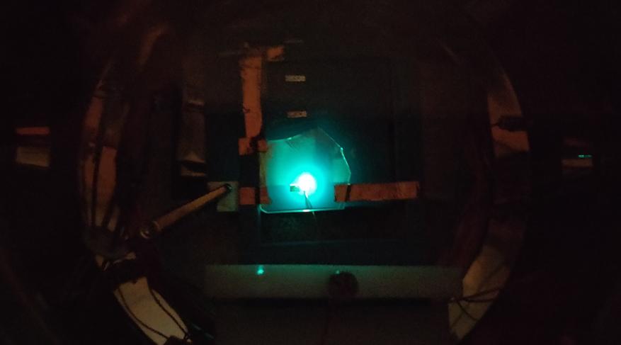
- An external collector (aluminum rod or phosphor screen) is held approximately 0.5 cm above device emitters. The aluminum collector is held at 100V while the phosphor screen is held at 1 kV to observe emitter current (see Figure 4).
- Keysight B2902A Source Measure Unit (SMU) and EasyEXPERT software to generate input voltage versus output current (I-V) curves.
Lifetime Testing Vacuum Chamber
- Capable of reaching UHV pressure (< 10-7 Torr) using Agilent Varian VacIon 300 StarCell Ion Pump.
- Devices are powered using a driver circuit that provides a constant square pulse from 0-40V at a low duty cycle of 20%.
- LabVIEW control system monitors temperature, pressure, and gate and emitter voltages and currents.
Test Procedure
When testing transistor devices inside a vacuum chamber, the following sequence of steps is followed:
- Clean vacuum chamber with isopropanol and place devices inside.
- Turn on turbo pump and wait for the pressure to drop below 10^-6 Torr.
- Set the temperature control to desired temperature.
- Lower the gate connection pin onto the gate pad.
- Use the EasyEXPERT software to power the collector to 100 V, sweep the gate voltage, and measure the output emitter-to-collector current to generate I-V curve. Repeat until experiments are complete.
- Turn off the temperature controller and wait for the temperature to drop to room temperature.
- Turn off the turbo pump and open the nitrogen gas valve to coat the vacuum chamber with nitrogen.
- Remove devices from chamber and place into their protective packaging. Separate any destroyed devices for failure observation.
Preliminary Testing
Preliminary tests are done to obtain I-V curves for the devices in a heated vacuum environment, prior to lifetime testing.
- Devices are heated up to 400 °C using a molybdenum heat chuck within the vacuum chamber.
- The collector voltage is held constant.
- The gate voltage is pulsed at a low duty cycle (5-20%) to prevent damage and swept up to a ~40V amplitude.
- The current through the collector and gate are measured by the SMU to assess gate leakage current in the devices.
Lifetime Testing
Lifetime tests are performed to analyze long term behavior and failure conditions of the devices.
- Devices are heated up to 400 °C.
- The gate voltage is pulsed at a fixed amplitude.
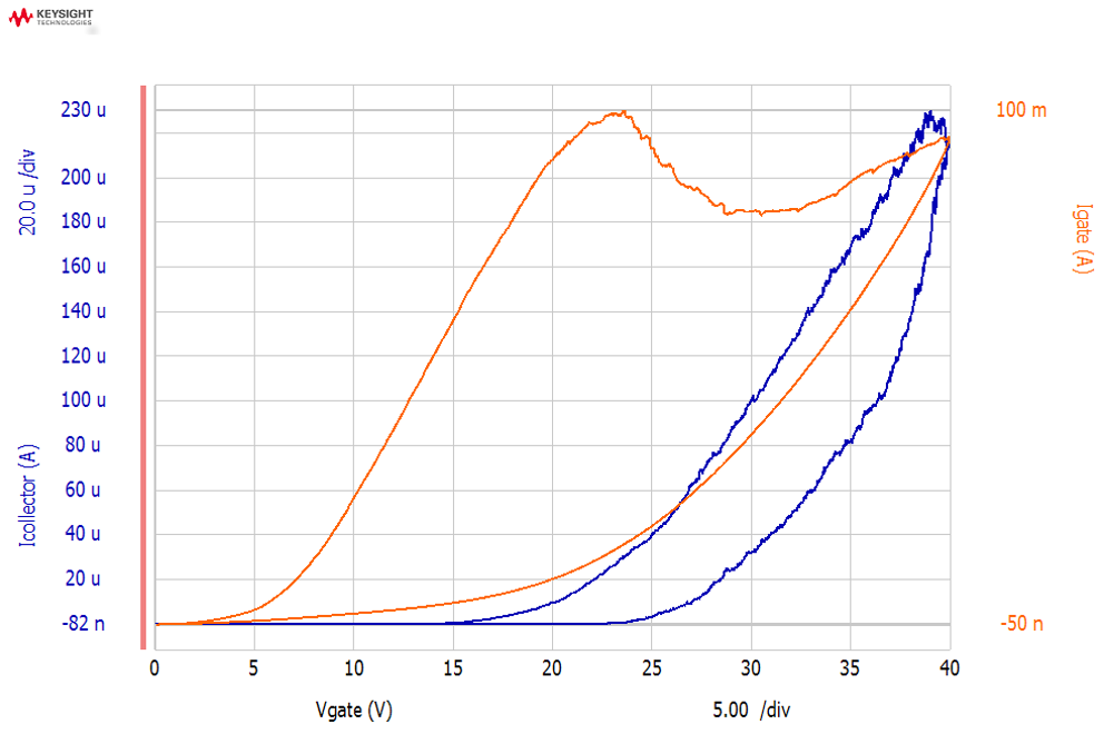
- LabVIEW control program takes periodic I-V curves observe the degradation of the device over hundreds of hours.
- LabVIEW monitors arcing from the gate to the emitter as charge builds in the gate dielectric. If multiple arcs occur, the system shuts down to prevent further damage and to allow for failure analysis
Results & Analysis
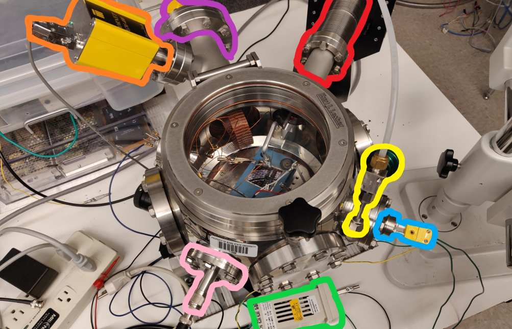
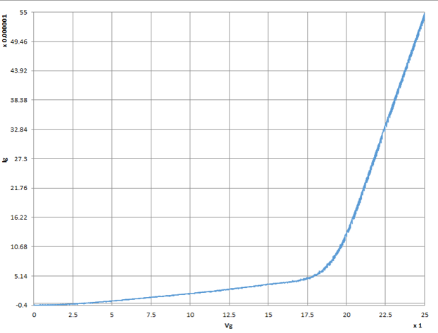
- The vertical emitter devices turned on at approximately 17 V.
- Emitter-collector current at a pulsed gate voltage of 40 V ranged from 20 uA to 65 uA, but some devices where the anode was positioned closer to the emitter produced up to 250 uA.
- Gate leakage current started in the 1 mA range – very high due to the large distance between anode and emitter array.
- As the device experienced repeated gate-emitter arcing, leakage current increased to the 50-120 mA range due to the gradual destruction of the gate dielectric (insulator).
- Many devices failed before making it to lifetime testing due to repeated arcing.
Conclusion
- By using a high vacuum chamber and a source measure unit, IV curves for three-terminal vertical field emitter devices were observed.
- However, due to the separation of the emitter and the non-ideal external collector, the devices suffered from high gate leakage current.
- The collected data is important for fabrication of future three-terminal devices that will have a collector built-in.
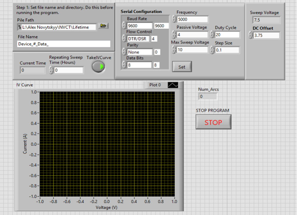
- The long-term goals for these devices is to reduce gate leakage current, prevent gate-emitter arcing, create a built-in collector, and to decrease collector-emitter spacing to the nanoscale range.
- Ideally, future I-V characteristics will replicate trends shown in Figure 6, as opposed to those shown in Figure 2.
- Finalized NVCT devices are intended to operate in the high temperature and radioactive environment of a nuclear reactor.
Material support for this work is provided by the Air Force Office of Scientific Research under grant FA9550-18-1-0436.
Additional Information
For questions or comments about this research, contact Oleksandr Novytskyy at oleksandrnovytskyy@boisestate.edu.