Blake Rapp
Graduate Research Assistant
Department of Electrical and Computer Engineering
Blake joined the Nanoscale Materials and Device Group at Boise State University in the middle of his sophomore year as an undergraduate student in Electrical and Computer Engineering in the beginning of 2009. He has previous degrees in Music Entertainment Management as well as Electronics and Computer Technology, both Associate’s degrees. Soon after obtaining his ECT degree Blake began working at Micron Technology, a semiconductor device manufacturer, as a technician repairing and testing various pieces of manufacturing equipment. Some of the equipment parts involved include various electric and pneumatic valves, mass flow controllers (MFCs), RF load matching networks, and wafer handling robots.
Blake initially started work with the Nanoscale Materials and Device Group as a part of the High-k Device Characterization team. Blake’s work involved exploring the electrical characteristics of different semiconductor devices at various temperatures (6-500K), the characteristics of Negative Bias Temperature Instability (NBTI) at cryogenic temperatures, as well as the electrical characteristics of novel nanoscale structures based on DNA.
In the Spring of 2012, Blake was accepted into the Master’s of Science program in the Electrical and Computer Engineering Department. As a part of this transition, Blake’s research focus has shifted to the study of optical and photonic phenomena associated with DNA based nano-devices. Darkfield spectroscopy is the primary vehicle for the study at this time.
Instruments and Techniques
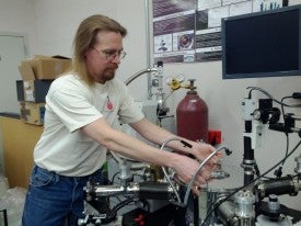
- Keithley 4200-SCS Semiconductor Characterization System
- Perform I-V measurements on various devices
- Connect to external equipment to perform other measurements:
- Capacitance-Voltage
- Conductance
- Low Temperature Probe Station
- Perform I-V and conductance measurements from cryogenic to room temperatures
- Agilent 4156C Precision Semiconductor Parameter Analyzer
- Perform I-V measurements on various devices
- Connect to external equipment to perform other measurements:
- Capacitance-Voltage
- Conductance
- Agilent 4284 Precision LCR
- Perform Capacitance-Voltage measurements
- Stanford Research Systems Model 830 DSP Lock-In Amplifier
- JEOL JEM-2100 HR Analytical Transmission Electron Microscope (TEM)
- Eppendorf Mastercycler – compact thermal cycler (4 to 99 oC)
- Eppendorf Biophotometer Plus – compact UV/Vis photometer
- Digital Instruments MultiMode SPM with a Nanoscope IV controller
- Peak Force tapping
- Bruker Dimension Icon Atomic Force Microscope
- Peak Force tapping
- Non-Contact tapping
Publications
Peer Reviewed Journal Publications
- William P. Klein, Charles N. Schmidt, Blake Rapp, Sadao Takabayashi, William B. Knowlton, Jeunghoon Lee, Bernard Yurke, William L. Hughes, Elton Graugnard, and Wan Kuang, Multiscaffold DNA Origami Nanoparticle Waveguides. (Nano Lett., 2013, 13 (8), pp. 3850 – 3856, http://dx.doi.org/10.1021/nl401879r)
Conference Publications
- Richard G. Southwick III, Shem T. Purnell**, Blake A. Rapp**, Ryan J. Thompson**, Shane K Pugmire**, Ben Kaczer, Tibor Grasser, and William B. Knowlton, Cryogenic to Room Temperature Effects of NBTI in High-K PMOS Devices, oral presentation and paper presentation at the IEEE International Integrated Reliability Workshop (Oct. 17-21, 2011)
Conference Presentations and Posters
- B. Rapp**, S. Purnell**, S. Pugmire**, R. Thompson**, R. Butler*, R. Southwick III, W. Knowlton, Thermal Effects of Light Exposure on pMOSFET Device Behavior, poster presentation at the 2011 Undergraduate Research and Scholarship Conference (Boise, Idaho; April 11, 2011)
- Shem T. Purnell**, Shane K Pugmire**, Blake A. Rapp**, Ryan J. Thompson**, Richard G. Southwick III, Tibor Grasser, Ben Kaczer, and William B. Knowlton, Comparison of Trends in Cryogenic Measurements of SiO2 and HfO2/SiO2 pMOSFETs, poster presentation at the IEEE International Integrated Reliability Workshop (Fallen Leaf Lake, CA; Oct. 16-20, 2011)
- Blake Rapp**, Christopher Buu*, Lejmarc Snowball**, Jason Brotherton, Nick Schmidt**, Amber Lay**, William B. Knowlton, Wan Kuang, William L. Hughes, Bernard Yurke, Elton Graugnard, Progress Toward the Synthesis and Electrical Characterization of Au-Functionalized DNA Origami Nanotubes, poster presentation at the IEEE International Integrated Reliability Workshop (Fallen Leaf Lake, CA; Oct. 16-20, 2011)
- Ryan J. Thompson**, Richard G. Southwick III, Blake A. Rapp**, Christopher Buu*, Amit Jain, and William B. Knowlton, New Applications of the Boise State Band Diagram Program, poster presentation at the IEEE International Integrated Reliability Workshop (Fallen Leaf Lake, CA; Oct. 16-20, 2011)
- Ryan J. Thompson**, Shem T. Purnell**, Blake A. Rapp**, Development of Sensors for Tracking Behavior of Wildlife, poster presentation at the 2012 Undergraduate Research and Scholarship Conference (Boise, Idaho; April 16, 2012)
- Amber Thompson**, Christopher Buu, Blake Rapp**, Jason Brotherton, Lejmarc Snowball, Nathan Robinson, Elton Graugnard, Bernard Yurke, Wan Kuang, Jeunghoon Lee, William L. Hughes, William B. Knowlton, Au-Functionalized DNA Origami Nanotubes Synthesis, Deposition, and Preliminary Electrical Charaterization, poster presentation at the 2012 Undergraduate Research and Scholarship Conference (Boise, Idaho; April 16, 20112)
- Sadao Takabayashi, William Klein, Blake Rapp, Elias Lindau**, Lejmarc Snowball**, Jeunghoon Lee, William B. Knowlton, Bernard Yurke, Elton Graugnard, Wan Kuang, William L. Hughes, Maximizing Nanoparticle Attachment onto DNA Origami Nanotubes, poster presentation at the Foundations of Nanoscience conference (FNANO) (Snowbird, Utah; April 14 – 19, 2013)
- William Klein, Charles Schmidt**, Blake Rapp, Sadao Takabayashi, William B. Knowlton, Elton Graugnard, Jeunghoon Lee, Bernard Yurke, William L. Hughes, Wan Kuang, DNA Origami Templated Self-Assembly for Nanophotonic Devices and Materials, presentation at the Foundations of Nanoscience conference (FNANO) (Snowbird, Utah; April 14 – 19, 2013)