Annalies G. Tipton, Karen Perez, Dr. Elton Graugnard, Dr. David Estrada
Introduction
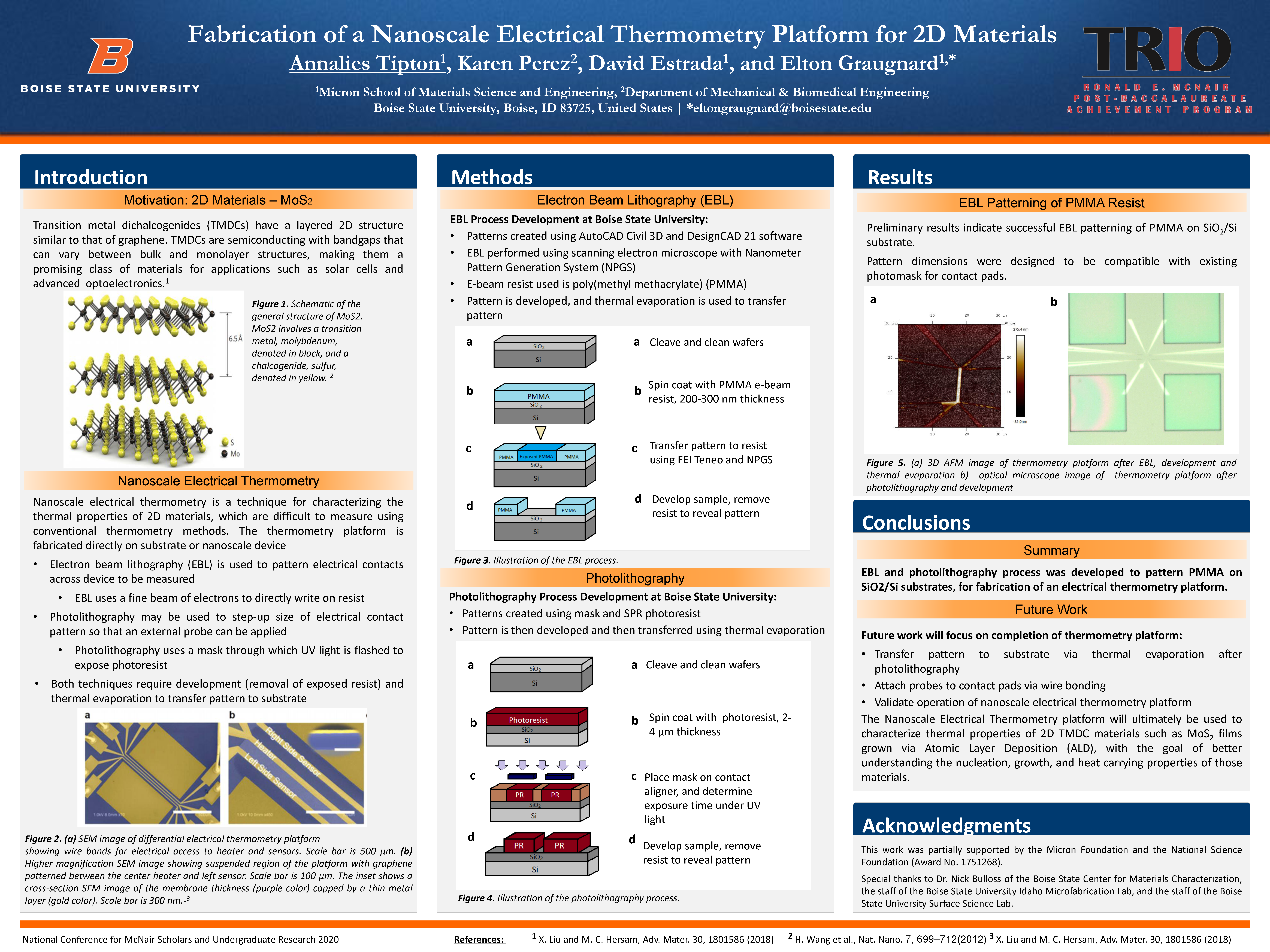
Motivation: 2D Materials – MoS2
Transition metal dichalcogenides (TMDCs) have a layered 2D structure similar to that of graphene. TMDCs are semiconducting with bandgaps that can vary between bulk and monolayer structures, making them a promising class of materials for applications such as solar cells and advanced optoelectronics.1
Nanoscale Electrical Thermometry
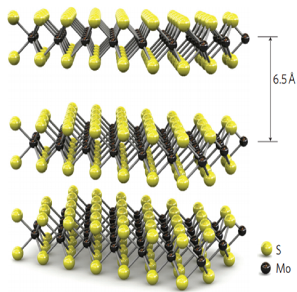
Nanoscale electrical thermometry is a technique for characterizing the thermal properties of 2D materials, which are difficult to measure using conventional thermometry methods. The thermometry platform is fabricated directly on substrate or nanoscale device
- Electron beam lithography (EBL) is used to pattern electrical contacts across device to be measured
- EBL uses a fine beam of electrons to directly write on resist
- Photolithography may be used to step-up size of electrical contact pattern so that an external probe can be applied
- Photolithography uses a mask through which UV light is flashed to expose photoresist
- Both techniques require development (removal of exposed resist) and thermal evaporation to transfer pattern to substrate
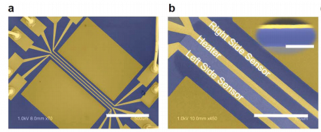
showing wire bonds for electrical access to heater and sensors. Scale bar is 500 μm. (b) Higher magnification SEM image showing suspended region of the platform with graphene patterned between the center heater and left sensor. Scale bar is 100 μm. The inset shows a cross-section SEM image of the membrane thickness (wider purple color) capped by a thin metal layer (thinner gold color). Scale bar is 300 nm.-3
Methods
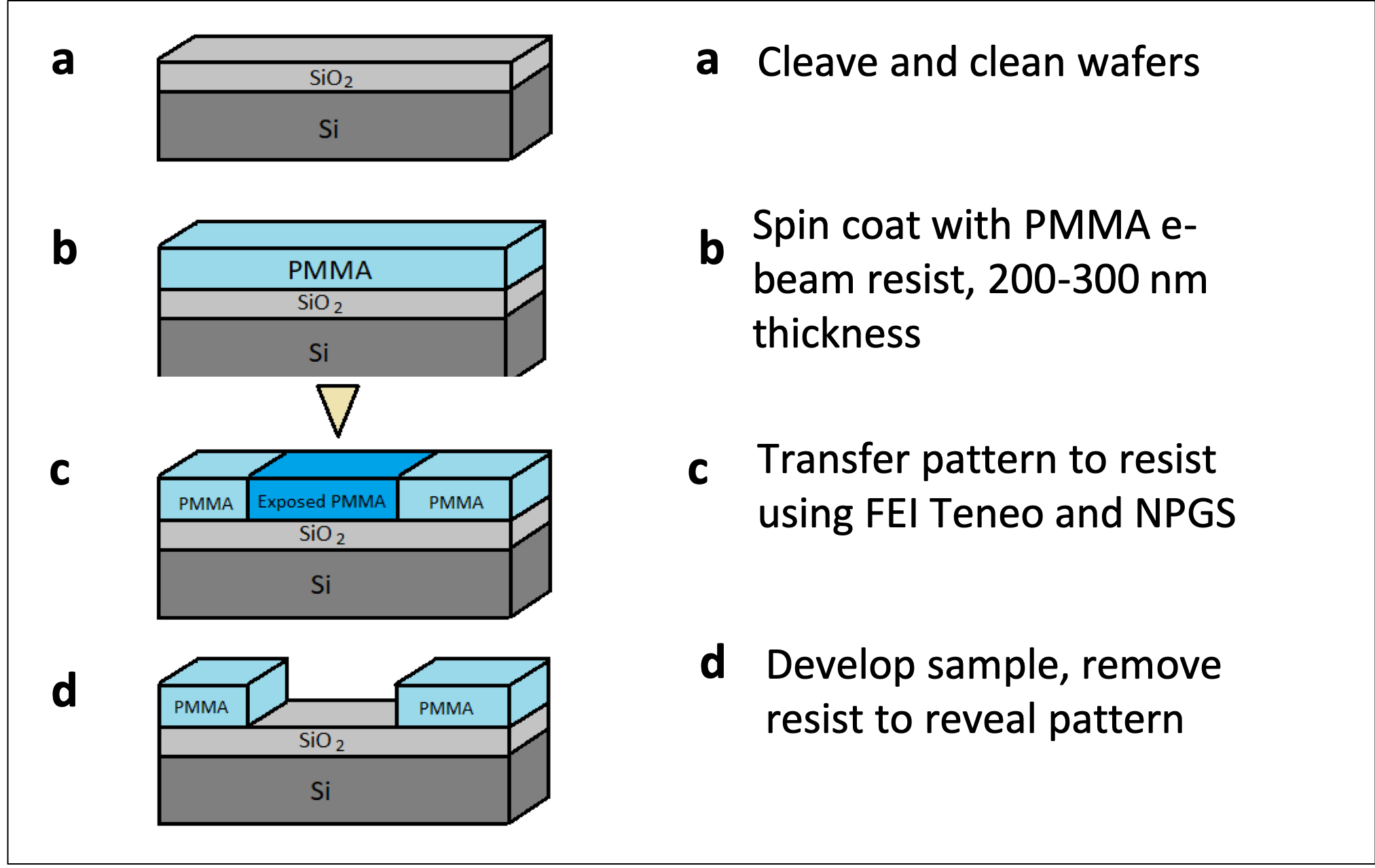
Electron Beam Lithography (EBL)
EBL Process Development at Boise State University:
- Patterns created using AutoCAD Civil 3D and DesignCAD 21 software
- EBL performed using scanning electron microscope with Nanometer Pattern Generation System (NPGS)
- E-beam resist used is poly(methyl methacrylate) (PMMA)
- Pattern is developed, and thermal evaporation is used to transfer pattern
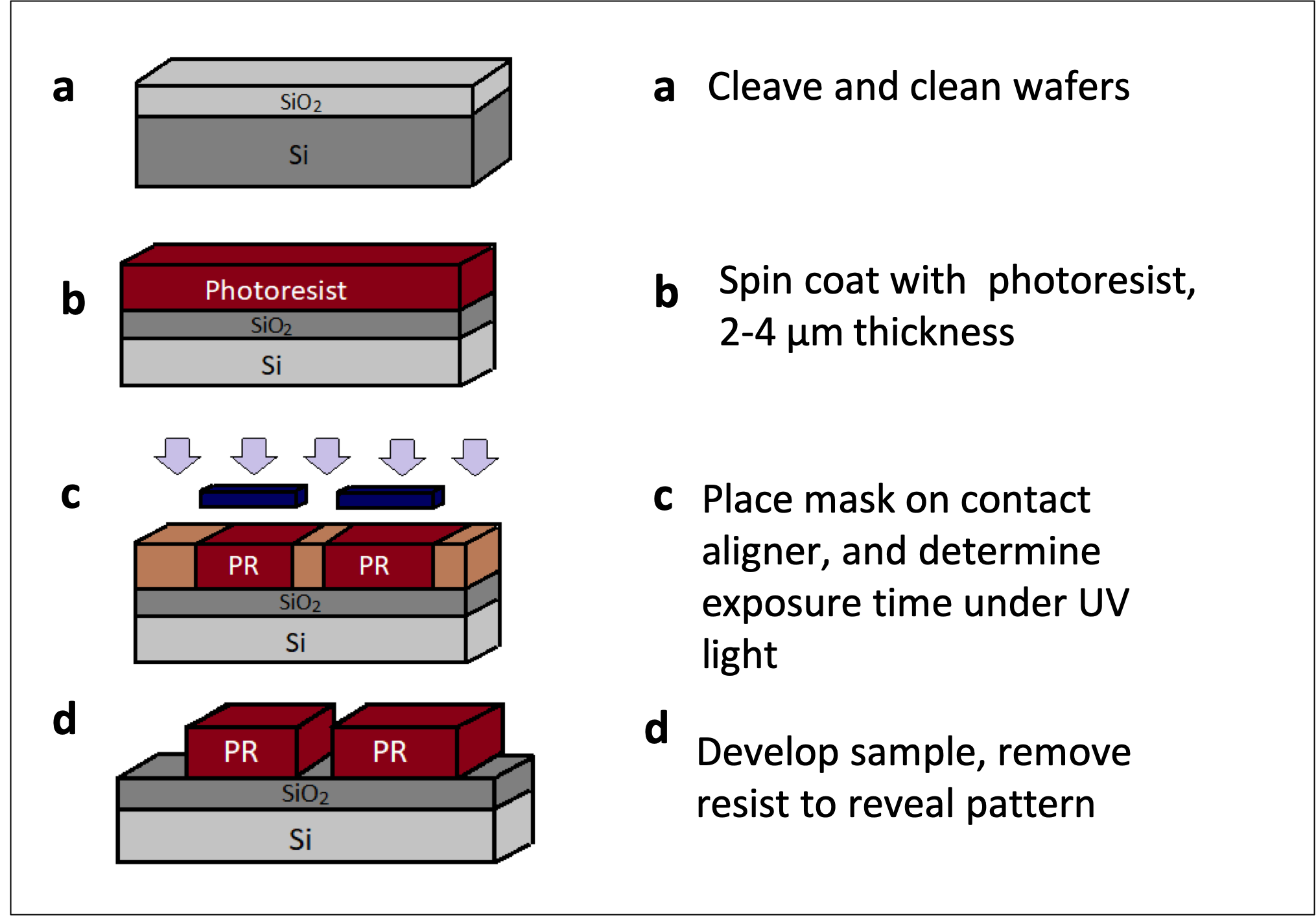
Photolithography
Photolithography Process Development at Boise State University:
- Patterns created using mask and SPR photoresist
- Pattern is then developed and then transferred using thermal evaporation
Results
EBL Patterning of PMMA Resist
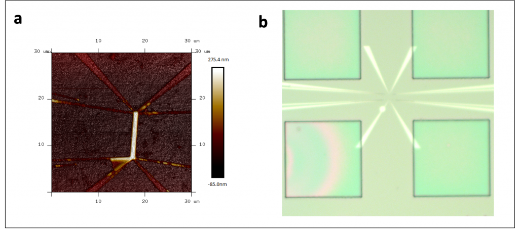
Preliminary results indicate successful EBL patterning of PMMA on SiO2/Si substrate.
Pattern dimensions were designed to be compatible with existing photomask for contact pads.
Conclusions
Summary
EBL and photolithography process was developed to pattern PMMA on SiO2/Si substrates, for fabrication of an electrical thermometry platform.
Future Work
Future work will focus on completion of thermometry platform:
- Transfer pattern to substrate via thermal evaporation after photolithography
- Attach probes to contact pads via wire bonding
- Validate operation of nanoscale electrical thermometry platform
The Nanoscale Electrical Thermometry platform will ultimately be used to characterize thermal properties of 2D TMDC materials such as MoS2 films grown via Atomic Layer Deposition (ALD), with the goal of better understanding the nucleation, growth, and heat carrying properties of those materials.
Acknowledgements
Special thanks to Dr. Nick Bulloss of the Boise State Center for Materials Characterization, the staff of the Boise State University Idaho Microfabrication Lab, and the staff of the Boise State University Surface Science Lab.
This work was partially supported by the Micron Foundation and the National Science Foundation (Award No. 1751268).
References
- X. Liu and M. C. Hersam, Adv. Mater. 30, 1801586 (2018)
- H. Wang et al., Nat. Nano. 7, 699–712(2012)
- X. Liu and M. C. Hersam, Adv. Mater. 30, 1801586 (2018)